


Rev.1.10 Jul 01, 2005 page 170 of 318
REJ09B0124-0110
M16C/6N Group (M16C/6NK, M16C/6NM) 14. Serial I/O
Under development
This document is under development and its contents are subject to change.
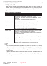
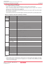
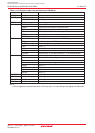
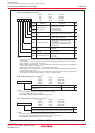
Item Specification
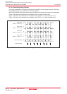
Transfer data format • Direct format
• Inverse format
Transfer clock • The CKDIR bit in the U2MR register = 0 (internal clock) : fi/ 16(n+1)
fi = f1SIO, f2SIO, f8SIO, f32SIO. n: Setting value of the U2BRG register 00h to FFh
• The CKDIR bit = 1 (external clock) : fEXT/16(n+1)
fEXT: Input from CLK2 pin. n: Setting value of the U2BRG register 00h to FFh
Transmission start condition Before transmission can start, the following requirements must be met
• The TE bit in the U2C1 register = 1 (transmission enabled)
• The TI bit in the U2C1 register = 0 (data present in the U2TB register)
Reception start condition Before reception can start, the following requirements must be met
• The RE bit in the U2C1 register = 1 (reception enabled)
• Start bit detection
• For transmission
When the serial I/O finished sending data from the U2TB transfer register (U2IRS bit = 1)
• For reception
When transferring data from the UART2 receive register to the U2RB register (at
completion of reception)
Error detection • Overrun error
(1)
This error occurs if the serial I/O started receiving the next data before reading the
U2RB register and received the bit one before the last stop bit of the next data
• Framing error
(3)
This error occurs when the number of stop bits set is not detected
• Parity error
(3)
During reception, if a parity error is detected, parity error signal is output from the
TXD2 pin.
During transmission, a parity error is detected by the level of input to the RXD2 pin
when a transmission interrupt occurs
• Error sum flag
This flag is set to “1” when any of the overrun, framing, and parity errors is encountered
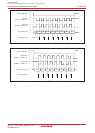
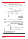
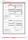
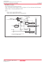
14.1.6 Special Mode 4 (SIM Mode) (UART2)
Based on UART mode, this is an SIM interface compatible mode. Direct and inverse formats can be
implemented, and this mode allows to output a low from the TXD2 pin when a parity error is detected.
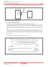
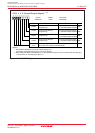
Table 14.17 lists the specifications of SIM mode. Table 14.18 lists the registers used in the SIM mode and
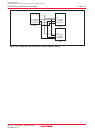
the register values set. Figure 14.32 shows the typical transmit/receive timing in SIM mode.
Table 14.17 SIM Mode Specifications
Interrupt request
generation timing
(2)
NOTES:
1. If an overrun error occurs, the value of the U2RB register will be indeterminate. The IR bit in the S2RIC
register does not change.
2. A transmit interrupt request is generated by setting the U2IRS bit in the U2C1 register to “1” (transmit is
completed) and U2ERE bit to “1” (error signal output) after reset. Therefore, when using SIM mode, set
the IR bit to “0” (interrupt not requested) after setting these bits.
3.The timing at which the framing error flag and the parity error flag are set is detected when data is
transferred from the UARTi receive register to the UiRB register.