


Rev.1.10 Jul 01, 2005 page 194 of 318
REJ09B0124-0110
M16C/6N Group (M16C/6NK, M16C/6NM) 15. A/D Converter
Under development
This document is under development and its contents are subject to change.
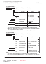
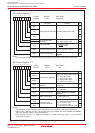
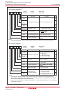
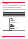
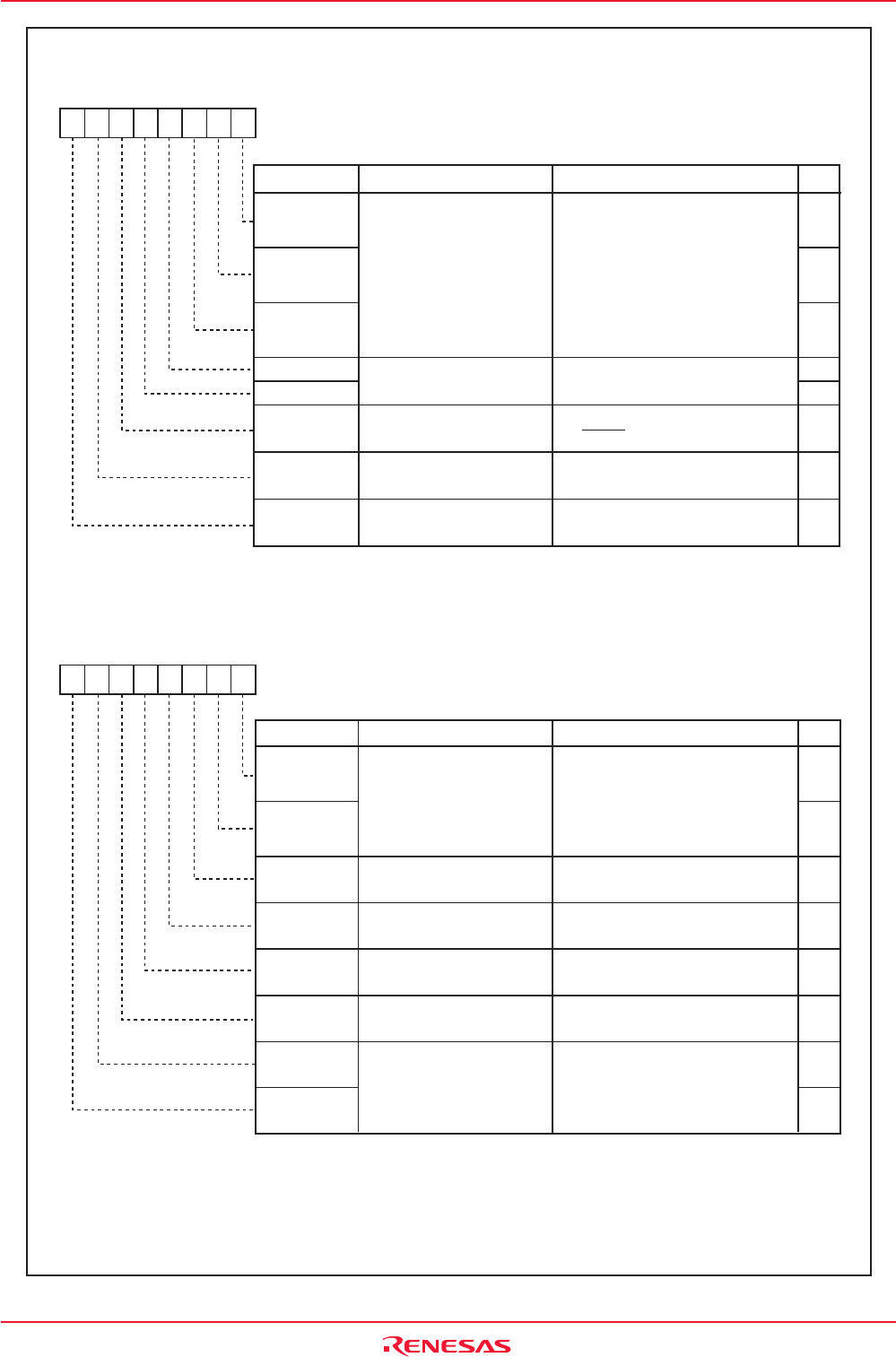
Figure 15.8 ADCON0 Register and ADCON1 Register in Repeat Sweep Mode 1
CH0
CH1
CH2
MD0
MD1
TRG
ADST
CKS0
1 1 : Repeat sweep mode 0 or
Repeat sweep mode 1
0 : Software trigger
1 : ADTRG trigger
0 : A/D conversion disabled
1 : A/D conversion started
Refer to NOTE 2 for ADCON2
Register
Trigger Select Bit
A/D Conversion Start Flag
Frequency Select Bit 0
Analog Input Pin Select Bit
A/D Operation Mode
Select Bit 0
A/D Control Register 0
(1)
b7 b6 b5 b4 b3 b2 b1 b0
Bit Symbol
Bit Name Function
RW
RW
RW
RW
RW
RW
RW
RW
RW
Invalid in repeat sweep mode 1
b4 b3
11
Symbol Address After Reset
ADCON0 03D6h 00000XXXb
NOTE:
1. If the ADCON0 register is rewritten during A/D conversion, the conversion result will be indeterminate.
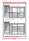
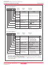
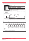
RW
RW
RW
RW
RW
RW
RW
RW
SCAN0
SCAN1
MD2
BITS
VCUT
OPA0
OPA1
CKS1
Bit Name Function
Bit Symbol
RW
0 : 8-bit mode
1 : 10-bit mode
Set to "1" when repeat sweep
mode 1 is selected
1 : VREF connected
Refer to NOTE 2 for ADCON2
Register
When repeat sweep mode 1 is selected
A/D Sweep Pin Select Bit
8/10-Bit Mode Select Bit
VREF Connect Bit
(3)
A/D Operation Mode
Select Bit 1
External Op-Amp
Connection Mode Bit
Frequency Select Bit 1
0 0 :
ANEX0 and ANEX1 are not used
0 1 : Do not set a value
1 0 : Do not set a value
1 1 :
External op-amp connection mode
b7 b6 b5 b4 b3 b2 b1 b0
A/D Control Register 1
(1)
b7 b6
0 0 : AN0 (1 pin)
0 1 : AN0, AN1 (2 pins)
1 0 : AN0 to AN2 (3 pins)
1 1 : AN0 to AN3 (4 pins)
(2)
b1 b0
11
Symbol Address After Reset
ADCON1 03D7h 00h
NOTES:
1. If the ADCON1 register is rewritten during A/D conversion, the conversion result will be indeterminate.
2. AN0_0 to AN_7, and AN2_0 to AN2_7 can be used in same way as AN0 to AN7. Use the ADGSEL1 to ADGSEL0
bits in the ADCON2 register to select the desired pin.
3. If the VCUT bit is reset from "0" (VREF unconnected) to "1" (VREF connected), wait for 1 µs or more before
starting A/D conversion.