


Rev.1.10 Jul 01, 2005 page 244 of 318
REJ09B0124-0110
M16C/6N Group (M16C/6NK, M16C/6NM) 20. Flash Memory Version
Under development
This document is under development and its contents are subject to change.
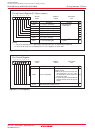
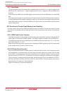
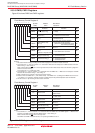
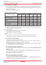
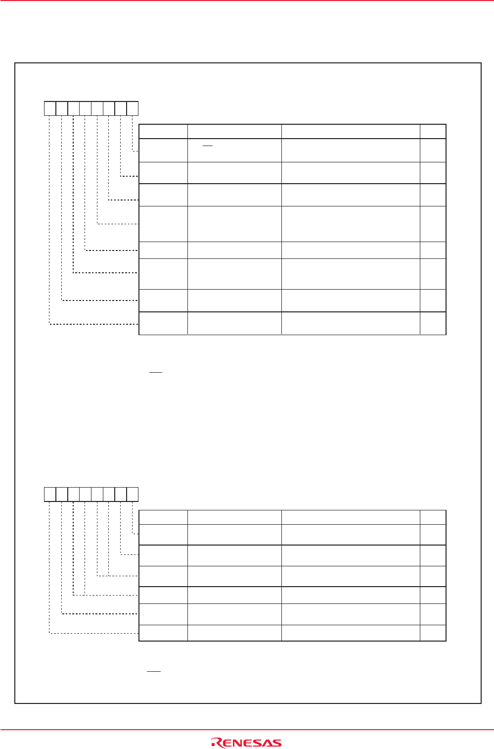
Figure 20.4 FMR0 Register and FMR1 Register
Flash Memory Control Register 0
Symbol Address After Reset
FMR0 01B7h 00000001b
b7 b6 b5 b4 b3 b2 b1 b0
0
RY/BY Status Flag
FMR00
0 : Busy (being written or erased)
(1)
1 : Ready
CPU Rewrite Mode
Select Bit
(2)
0 : Disables CPU rewrite mode
1 : Enables CPU rewrite mode
FMR01
0 : Boot ROM area is accessed
1 : User ROM area is accessed
Lock Bit Disable Select
Bit
(3)
0: Enables lock bit
1: Disables lock bit
Flash Memory Stop
Bit
(4) (5)
0 Enables flash memory operation
1: Stops flash memory operation
(placed in low power dissipation mode,
flash memory initialized)
User ROM Area Select
Bit
(4)
(Effective in only boot mode)
FMR02
FMSTP
FMR05
Set to "0"Reserved Bit
Program Status Flag
(6)
FMR06
Erase Status Flag
(6)
FMR07
0 : Terminated normally
1 : Terminated in error
0 : Terminated normally
1 : Terminated in error
RW
RW
RW
RW
RW
RO
RO
-
(b4)
RW
RO
NOTES:
1.This status includes writing or reading with the lock bit program or read lock bit status command.
2.To set this bit to "1", write "0" and then "1" in succession. Make sure no interrupts or no DMA transfers will occur
before writing "1" after writing "0".
Write to this bit when the NMI pin is in the high state. Also, while in EW0 mode, write to this bit from a program in
other than the flash memory.
To set this bit to "0", in a read array mode.
3. To set this bit to "1", write "0" and then "1" in succession when the FMR01 bit = 1. Make sure no interrupts or no DMA
transfers will occur before writing "1" after writing "0".
4. Write to this bit from a program in other than the flash memory.
5. Effective when the FMR01 bit = 1 (CPU rewrite mode). If the FMR01 bit = 0, although the FMSTP bit can be set to
"1" by writing "1" in a program, the flash memory is neither placed in low power dissipation state nor initialized.
6. This bit is set to "0" by executing the clear status command.
Bit Symbol
Bit Name Function
Flash Memory Control Register 1
Symbol Address After Reset
FMR1 01B5h 0X00XX0Xb
b7 b6 b5 b4 b3 b2 b1 b0
000
EW1 Mode Select Bit
(1)
0 : EW0 mode
1 : EW1 mode
FMR11
Lock Bit Status Flag
FMR16
0 : Lock
1 : Unlock
RW
RO
Set to "0"Reserved Bit
RW
-
(b7)
Set to "0"Reserved Bit
RW
-
(b5-b4)
The value in this bit when read is
indeterminate.
Reserved Bit
RO
-
(b3-b2)
The value in this bit when read is
indeterminate.
Reserved Bit
-
(b0)
RW
RO
NOTE:
1. To set this bit to "1", write "0" and then "1" in succession when the FMR01 bit in the FMR0 register = 1. Make sure no
interrupts or no DMA transfers will occur before writing "1" after writing "0".
Write to this bit when the NMI pin is in the high state.
The FMR01 and FMR11 bits both are set to "0" by setting the FMR01 bit to "0".
Bit Symbol
Bit Name Function
20.3.3 FMR0, FMR1 Registers
Figure 20.4 shows FMR0 and FMR1 registers.