


Rev.1.10 Jul 01, 2005 page 196 of 318
REJ09B0124-0110
M16C/6N Group (M16C/6NK, M16C/6NM) 15. A/D Converter
Under development
This document is under development and its contents are subject to change.
15.2.5 Current Consumption Reducing Function
When not using the A/D converter, its resistor ladder and reference voltage input pin (VREF) can be
separated using the VCUT bit in the ADCON1 register. When separated, no current will flow from the
VREF pin into the resistor ladder, helping to reduce the power consumption of the chip.
To use the A/D converter, set the VCUT bit to “1” (VREF connected) and then set the ADST bit in the
ADCON0 register to “1” (A/D conversion start). The VCUT and ADST bits cannot be set to “1” at the same time.
Nor can the VCUT bit be set to “0” (VREF unconnected) during A/D conversion.
Note that this does not affect VREF for the D/A converter (irrelevant).
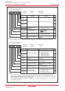
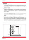
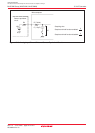
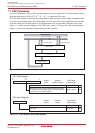
15.2.6 Output Impedance of Sensor under A/D Conversion
To carry out A/D conversion properly, charging the internal capacitor C shown in Figure 15.10 has to be
completed within a specified period of time. T (sampling time) as the specified time. Let output impedance
of sensor equivalent circuit be R0, microcomputer’s internal resistance be R, precision (error) of the A/D
converter be X, and the A/D converter’s resolution be Y (Y is 1024 in the 10-bit mode, and 256 in the 8-bit mode).
VC is generally VC = VIN {1 – e}
And when t = T, VC=VIN – VIN=VIN(1 – )
e =
– T= ln
Hence, R0 = –– R
Figure 15.10 shows analog input pin and external sensor equivalent circuit.
When the difference between VIN and VC becomes 0.1LSB, we find impedance R0 when voltage
between pins VC changes from 0 to VIN-(0.1/1024) VIN in time T. (0.1/1024) means that A/D precision
drop due to insufficient capacitor charge is held to 0.1LSB at time of A/D conversion in the 10-bit mode.
Actual error however is the value of absolute precision added to 0.1LSB. When f(XIN) = 10 MHz, T = 0.3
µs in the A/D conversion mode with sample & hold. Output impedance R0 for sufficiently charging capacitor
C within time T is determined as follows.
T = 0.3 µs, R = 7.8 kΩ, C = 1.5 pF, X = 0.1, and Y = 1024. Hence,
R0 = ––7.8 ✕10
3
13.9 ✕ 10
3
Thus, the allowable output impedance of the sensor circuit capable of thoroughly driving the A/D converter
turns out to be approximately 13.9 kΩ.
C (R0 + R)
1
1
Y
X
Y
X
Y
X
Y
X
C • ln
T
Y
X
1.5 ✕ 10
–12
• ln
1024
0.1
0.3 ✕ 10
-6
C (R0 + R)
–
t
T
C (R0 + R)
1
–