


Rev.1.10 Jul 01, 2005 page 257 of 318
REJ09B0124-0110
M16C/6N Group (M16C/6NK, M16C/6NM) 20. Flash Memory Version
Under development
This document is under development and its contents are subject to change.
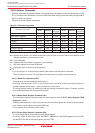
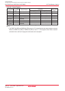
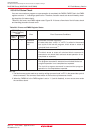
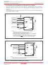
FRM00 Register
(Status Register)
Status
Error Error Occurrence Conditions
FMR07 bit FMR06 bit
(SR5) (SR4)
1 1 Command • Command is written incorrectly
Sequence • A value other than “xxD0h” or “xxFFh” is written in the second
error bus cycle of the lock bit program, block erase or erase all
unlocked block command
(1)
1 0 Erase error • The block erase command is executed on a locked block
(2)
• The block erase or erase all unlocked block command is
executed on an unlock block and auto erase operation is not
completed as expected
0 1 Program error • The program command is executed on locked blocks
(2)
• The program command is executed on unlocked blocks but
program operation is not completed as expected
• The lock bit program command is executed but program
operation is not completed as expected
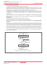
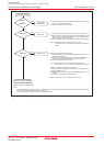
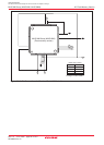
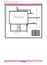
20.3.8 Full Status Check
If an error occurs when a program or erase operation is completed, the FMR06, FMR07 bits in the FMR0
register are set to “1”, indicating a specific error. Therefore, execution results can be confirmed by check-
ing these bits (full status check).
Table 20.6 lists errors and FMR0 register state. Figure 20.12 shows a flow chart of the full status check
and handling procedure for each error.
Table 20.6 Errors and FMR0 Register Status
NOTES:
1. The flash memory enters read array mode by writing command code “xxFFh” in the second bus cycle of
these commands. The command code written in the first bus cycle becomes invalid.
2. When the FMR02 bit in the FMR0 register is set to “1” (lock bit disabled), no error occurs even under
the conditions above.