


Rev.1.10 Jul 01, 2005 page 139 of 318
REJ09B0124-0110
M16C/6N Group (M16C/6NK, M16C/6NM) 14. Serial I/O
Under development
This document is under development and its contents are subject to change.
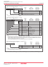
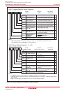
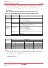
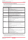
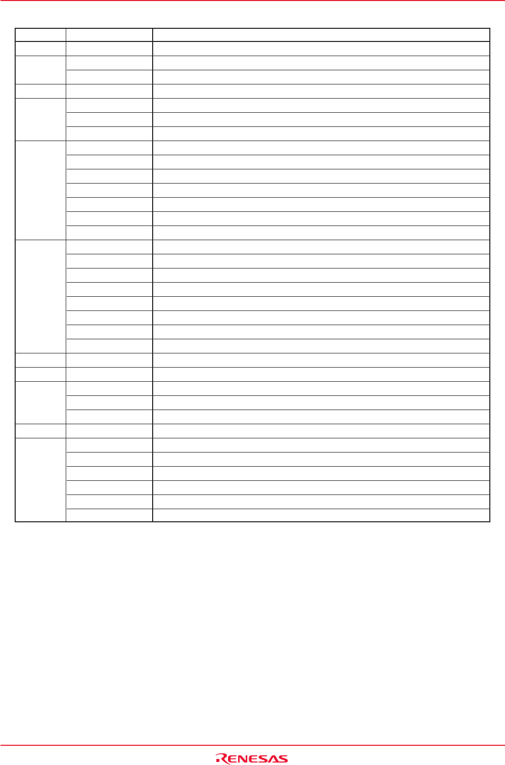
Table 14.2 Registers to Be Used and Settings in Clock Synchronous Serial I/O Mode
Register Bit Function
UiTB
(1)
0 to 7 Set transmission data
UiRB
(1)
0 to 7 Reception data can be read
OER Overrun error flag
UiBRG 0 to 7 Set a transfer rate
UiMR
(1)
SMD2 to SMD0 Set to “001b”
CKDIR Select the internal clock or external clock
IOPOL Set to “0”
UiC0 CLK1 to CLK0 Select the count source for the UiBRG register
CRS
_______ _______
Select CTS or RTS to use
TXEPT Transmit register empty flag
CRD
_______ _______
Enable or disable the CTS or RTS function
NCH Select TXDi pin output mode
CKPOL Select the transfer clock polarity
UFORM Select the LSB first or MSB first
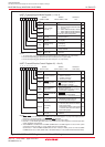
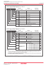
UiC1 TE Set this bit to “1” to enable transmission/reception
TI Transmit buffer empty flag
RE Set this bit to “1” to enable reception
RI Reception complete flag
U2IRS
(2)
Select the source of UART2 transmit interrupt
U2RRM
(2)
Set this bit to “1” to use continuous receive mode
UiLCH Set this bit to “1” to use inverted data logic
UiERE Set to “0”
UiSMR 0 to 7 Set to “0”
UiSMR2 0 to 7 Set to “0”
UiSMR3 0 to 2 Set to “0”
NODC Select clock output mode
4 to 7 Set to “0”
UiSMR4 0 to 7 Set to “0”
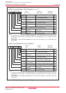
UCON U0IRS, U1IRS Select the source of UART0/UART1 transmit interrupt
U0RRM, U1RRM Set this bit to “1” to use continuous receive mode
CLKMD0 Select the transfer clock output pin when the CLKMD1 bit = 1
CLKMD1 Set this bit to “1” to output UART1 transfer clock from two pins
RCSP
_________
Set this bit to “1” to accept as input the UART0 CTS0 signal from the P6_4 pin
7 Set to “0”
i = 0 to 2
NOTES:
1.Not all register bits are described above. Set those bits to “0” when writing to the registers in clock
synchronous serial I/O mode.
2.Set the bit 4 and bit 5 in the U0C1 and U1C1 registers to “0”. The U0IRS, U1IRS, U0RRM and
U1RRM bits are in the UCON register.