


Rev.1.10 Jul 01, 2005 page 205 of 318
REJ09B0124-0110
M16C/6N Group (M16C/6NK, M16C/6NM) 18. CAN Module
Under development
This document is under development and its contents are subject to change.
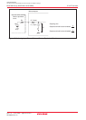
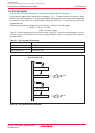
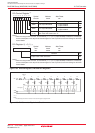
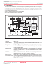
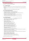
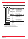
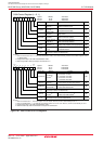
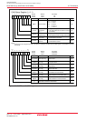
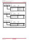
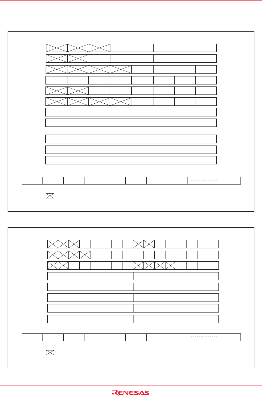
Figures 18.2 and 18.3 show the bit mapping in each slot in byte access and word access. The content of
each slot remains unchanged unless transmission or reception of a new message is performed.
Figure 18.2 Bit Mapping in Byte Access
Figure 18.3 Bit Mapping in Word Access
NOTE:
1. When is read, the value is the one written upon the transmission slot configuration.
The value is "0" when read on the reception slot configuration.
SID10 SID9 SID8 SID7 SID6
SID5 SID4 SID3 SID2 SID1 SID0
EID17 EID16 EID15 EID14
EID13 EID12
EID11
EID10
EID9 EID8 EID7 EID6
EID5 EID4 EID3 EID2 EID1 EID0
DLC3 DLC2 DLC1 DLC0
CAN Data Frame:
SID10 to 6 SID5 to 0 EID17 to 14 EID13 to 6 EID5 to 0 DLC3 to 0
Data Byte 0 Data Byte 1 Data Byte 7
Data Byte 0
Data Byte 1
Data Byte 7
Time Stamp high-order byte
Time Stamp low-order byte
b7 b0
SID10 SID9 SID8 SID7 SID6 SID5 SID4 SID3 SID2 SID1 SID0
EID17 EID16 EID15 EID14 EID13 EID12 EID11EID10 EID9 EID8 EID7 EID6
EID5 EID4 EID3 EID2 EID1 EID0 DLC3 DLC2 DLC1 DLC0
CAN Data Frame:
SID10 to 6 SID5 to 0 EID17 to 14 EID13 to 6 EID5 to 0 DLC3 to 0
Data Byte 0 Data Byte 1 Data Byte 7
Data Byte 0
Time Stamp high-order byte
Data Byte 2
Data Byte 4
Data Byte 6
Data Byte 1
Time Stamp low-order byte
Data Byte 3
Data Byte 5
Data Byte 7
b15 b0b8 b7
NOTE:
1. When is read, the value is the one written upon the transmission slot configuration.
The value is "0" when read on the reception slot configuration.