


Rev.1.10 Jul 01, 2005 page 229 of 318
REJ09B0124-0110
M16C/6N Group (M16C/6NK, M16C/6NM) 19. Programmable I/O Ports
Under development
This document is under development and its contents are subject to change.
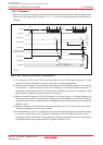
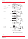
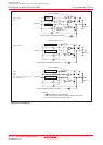
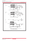
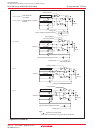
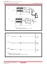
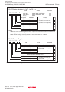
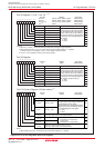
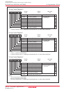
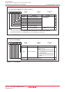
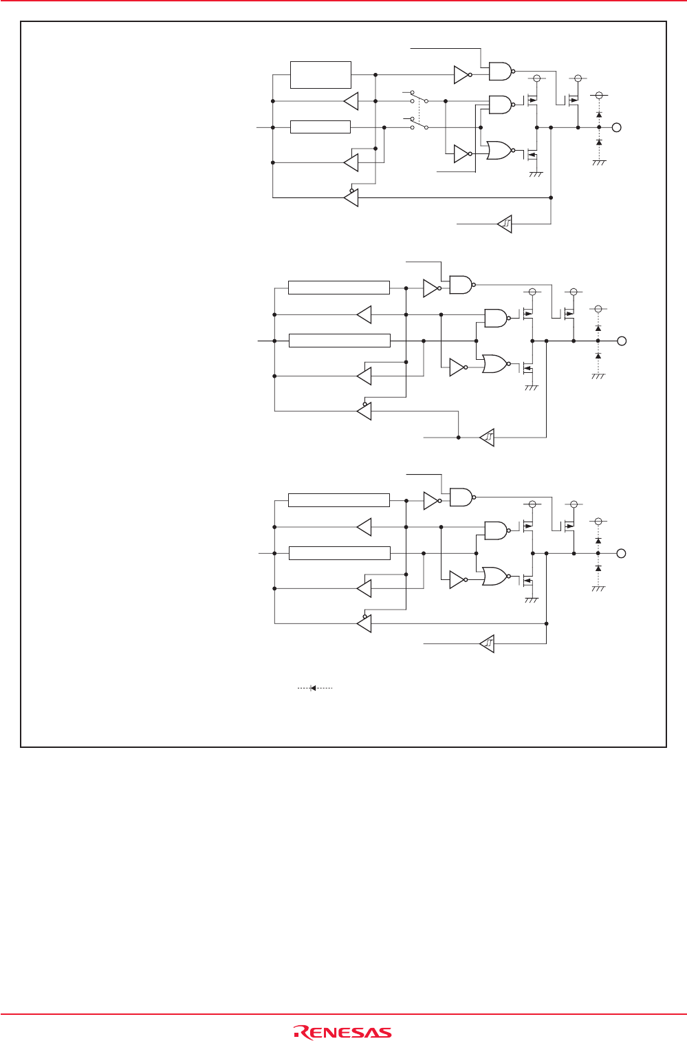
Figure19.2 I/O Ports (2)
"1"
Output
Data bus
Direction
register
Port latch
Pull-up selection
(NOTE 1)
Input to respective peripheral functions
Switching
between
CMOS and
Nch
(NOTE 1)
Data bus
Pull-up selection
Direction register
Port latch
Input to respective peripheral functions
Data bus
Pull-up selection
Direction register
Port latch
Input to respective peripheral functions
(NOTE 1)
NOTES:
1. Symbolizes a parasitic diode.
Make sure the input voltage on each port will not exceed VCC.
2. P11 to P13 are only in the 128-pin version.
P6_1, P6_5
P7_2
P8_2 to P8_4
P5_5
P7_7
P9_7
P11_0, P11_1, P11_5, P11_7
(2)
P13_5 to P13_7
(2)