


Rev.1.10 Jul 01, 2005 page 140 of 318
REJ09B0124-0110
M16C/6N Group (M16C/6NK, M16C/6NM) 14. Serial I/O
Under development
This document is under development and its contents are subject to change.
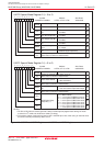
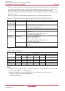
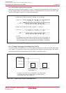
Table 14.3 lists the functions of the input/output pins during clock synchronous serial I/O mode. Table
14.3 shows pin functions for the case where the multiple transfer clock output pin select function is
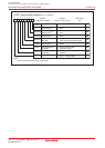
deselected. Table 14.4 lists the P6_4 pin functions during clock synchronous serial I/O mode.
Note that for a period from when the UARTi operation mode is selected to when transfer starts, the TXDi
pin outputs an “H”.
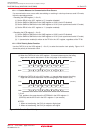
Figure 14.11 shows the transmit/receive timings during clock synchronous serial I/O mode.
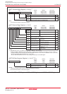
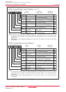
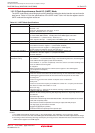
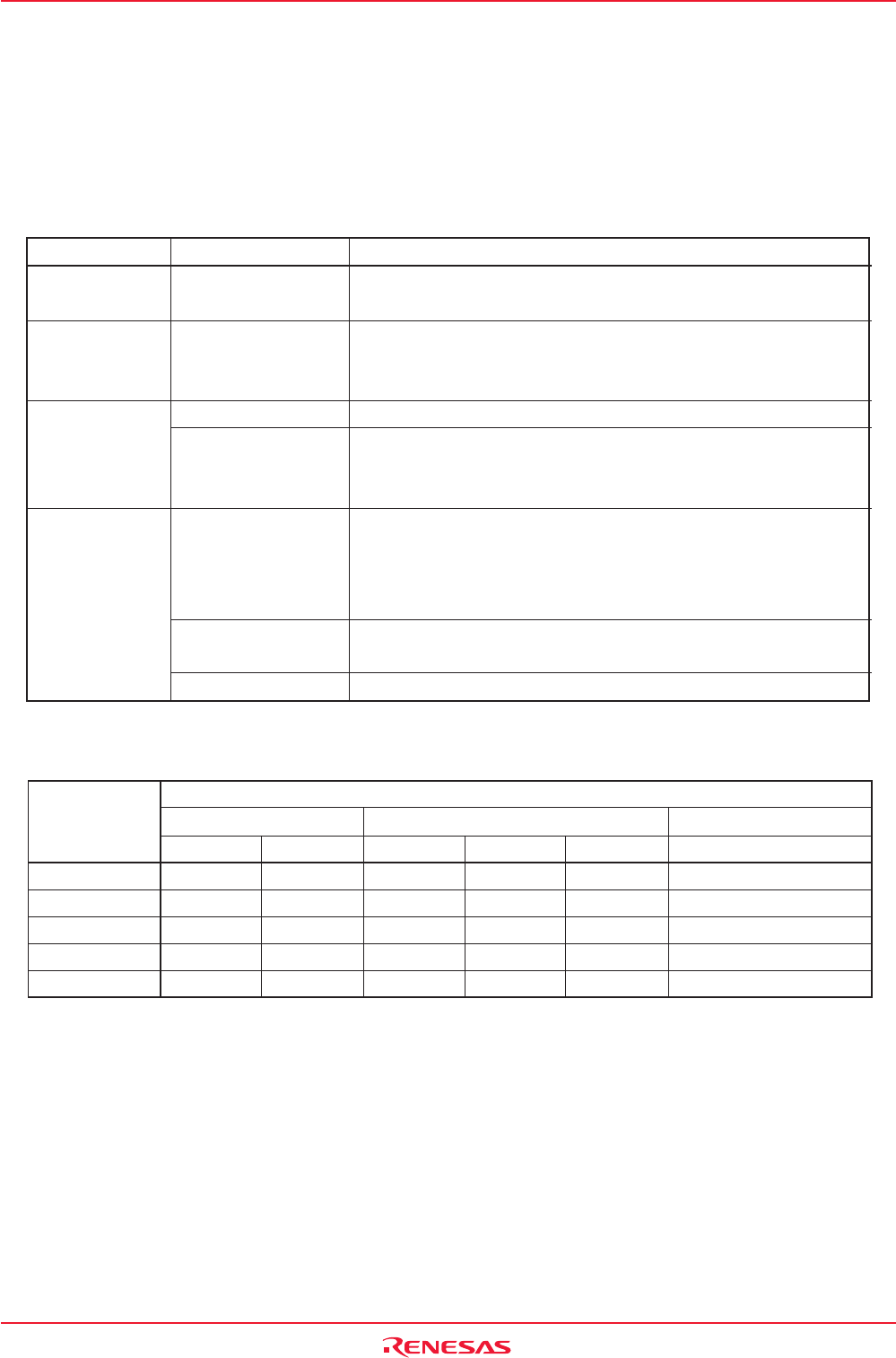
Table 14.3 Pin Functions (When Not Select Multiple Transfer Clock Output Pin Function)
i = 0 to 2
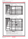
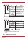
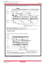
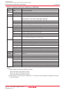
Table 14.4 P6_4 Pin Functions
TXDi
(P6_3, P6_7, P7_0)
RXDi
(P6_2, P6_6, P7_1)
CLKi
(P6_1, P6_5, P7_2)
_________________
CTSi/RTSi
(P6_0, P6_4, P7_3)
Pin Name Function Method of Selection
Serial Data Output
Serial Data Input
Transfer Clock Output
Transfer Clock Input
________
CTS Input
________
RTS Output
I/O Port
(Outputs dummy data when performing reception only)
PD6_2 and PD6_6 bits in PD6 register = 0
PD7_1 bit in PD7 register = 0
(Can be used as an input port when performing transmission only)
CKDIR bit in UiMR register = 0
CKDIR bit = 1
PD6_1 and PD6_5 bits in PD6 register = 0
PD7_2 bit in PD7 register = 0
CRD bit in UiC0 register = 0
CRS bit in UiC0 register = 0
PD6_0 and PD6_4 bits in PD6 register = 0
PD7_3 bit in PD7 register = 0
CRD bit = 0
CRS bit = 1
CRD bit = 1
-: “0” or “1”
NOTES:
1.
__________ __________
In addition to this, set the CRD bit in the U0C0 register to “0” (CTS0/RTS0 enabled) and the CRS
__________
bit in the U0C0 register to “1” (RTS0 selected).
2. When the CLKMD1 bit = 1 and the CLKMD0 bit = 0, the following logic levels are output:
• High if the CLKPOL bit in the U1C0 register = 0
• Low if the CLKPOL bit = 1
Bit set Value
Pin Function U1C0 Register UCON Register PD6 Register
CRD bit CRS bit RCSP bit CLKMD1 bit CLKMD0 bit PD6_4 bit
P6_4 1 - 0 0 - Input: 0, Output: 1
_________
CTS1 0 0 0 0 - 0
_________
RTS1 0 1 0 0 - -
_________
CTS0
(1)
0010- 0
CLKS1 - - - 1
(2)
1-