


Rev.1.10 Jul 01, 2005 page 157 of 318
REJ09B0124-0110
M16C/6N Group (M16C/6NK, M16C/6NM) 14. Serial I/O
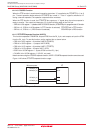
Under development
This document is under development and its contents are subject to change.
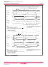
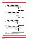
No acknowledgment detection
(NACK)
Rising edge of SCLi 9th bit
Acknowledgment detection (ACK)
Rising edge of SCLi 9th bit
Rising edge of SCLi 9th bit
L
Acknowledgment detection (ACK)
UARTi transmission
Falling edge of
SCLi next to the
9th bit
Falling and rising
edges of SCLi 9th
bit
L
1st to 8th bits are
stored into bit 7 to bit
0 in UiRB register
(3)
Bit 6 to bit 0 in the UiRB
register
(4)
are read as bit
7 to bit 1. Bit 8 in the UiRB
register is read as bit 0.
UARTi transmission
Rising edge of
SCLi 9th bit
Falling edge of
SCLi 9th bit
H
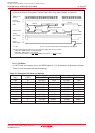
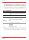
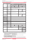
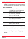
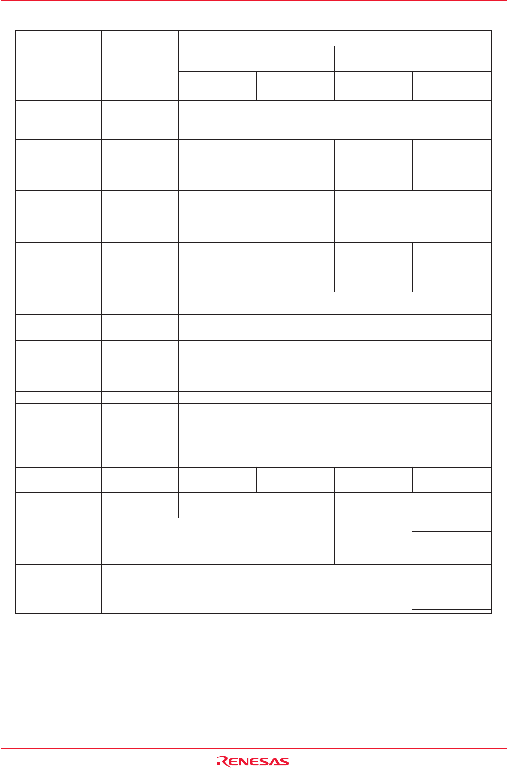
Table 14.12 I
2
C Mode Functions
i = 0 to 2
NOTES:
1. If the source or cause of any interrupt is changed, the IR bit in the interrupt control register for the changed interrupt may
inadvertently be set to “1” (interrupt requested). (Refer to 22.7 Interrupts.)
If one of the bits shown below is changed, the interrupt source, the interrupt timing, etc. change. Therefore, always be sure to set
the IR bit to “0” (interrupt not requested) after changing those bits.
• SMD2 to SMD0 bits in UiMR register • IICM bit in UiSMR register
• IICM2 bit in UiSMR2 register • CKPH bit in UiSMR3 register
2. Set the initial value of SDAi output while the SMD2 to SMD0 bits in the UiMR register = 000b (serial I/O disabled).
3. Second data transfer to the UiRB register (rising edge of SCLi 9th bit)
4. First data transfer to the UiRB register (falling edge of SCLi 9th bit)
5. See Figure 14.26 STSPSEL Bit Functions.
6. See Figure 14.24 Transfer to UiRB Register and Interrupt Timing.
7. When using UART0, be sure to set the IFSR06 bit in the IFSR0 register to “1” (cause of interrupt: UART0 bus collision detection).
When using UART1, be sure to set the IFSR07 bit in the IFSR0 register to “1” (cause of interrupt: UART1 bus collision detection).
Function
Clock
Synchronous
Serial I/O Mode
(SMD2 to SMD0 =
001b, IICM = 0)
I
2
C Mode (SMD2 to SMD0 = 010b, IICM = 1)
IICM2 = 0
(NACK/ACK interrupt)
IICM2 = 1
(UART transmit/receive interrupt)
CKPH = 0
(No clock delay)
CKPH = 1
(Clock delay)
Factor of Interrupt
Number 6, 7 and
10
(1) (5) (7)
Factor of Interrupt
Number 15, 17 and
19
(1) (6)
Factor of Interrupt
Number 16, 18 and
20
(1) (6)
Timing for Transferring
Data from UART
Reception Shift Register
to UiRB Register
UARTi Transmission
Output Delay
Functions of P6_3,
P6_7 and P7_0 Pins
Functions of P6_2,
P6_6 and P7_1 Pins
Functions of P6_1,
P6_5 and P7_2 Pins
Noise Filter Width
Read RXDi and
SCLi Pins Levels
Initial Value of TXDi
and SDAi Outputs
Initial and End
Value of SCLi
DMA1 Factor
(6)
Store Received
Data
Read Received
Data
-
UARTi transmission
Transmission started
or completed
(selected by UiIRS)
UARTi reception
When 8th bit received
CKPOL = 0 (rising edge)
CKPOL = 1 (falling edge)
CKPOL = 0 (rising edge)
CKPOL = 1 (falling edge)
Not delayed
TXDi output
RXDi input
CLKi input or
output selected
15 ns
Possible when the
corresponding port
direction bit = 0
CKPOL = 0 (H)
CKPOL = 1 (L)
-
UARTi reception
The UiRB register status is read
CKPH = 0
(No clock delay)
CKPH = 1
(Clock delay)
1st to 8th bits of the received data are stored into bit
7 to bit 0 in the UiRB register
Start condition detection or stop condition detection
(See Table 14.13 STSPSEL Bit Functions)
UARTi reception
Falling edge of SCLi 9th bit
Delayed
SDAi input/output
SCLi input/output
- (Cannot be used in I
2
C mode)
200 ns
Always possible no matter how the corresponding port direction bit is set
The value set in the port register before setting I
2
C mode
(2)
H
UARTi reception
Falling edge of SCLi 9th bit
1st to 7th bits of the received data are stored into
bit 6 to bit 0 in the UiRB
register, 8th bit is stored into
bit 8 in the UiRB register