


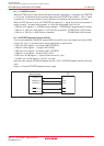
Rev.1.10 Jul 01, 2005 page 148 of 318
REJ09B0124-0110
M16C/6N Group (M16C/6NK, M16C/6NM) 14. Serial I/O
Under development
This document is under development and its contents are subject to change.
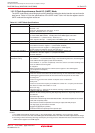
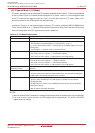
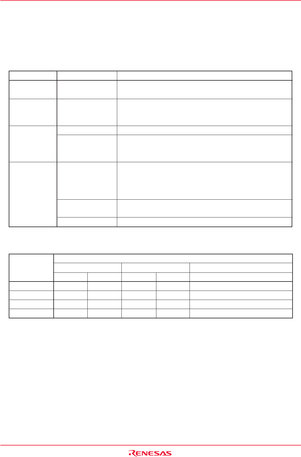
Table 14.7 lists the functions of the input/output pins during UART mode. Table 14.8 lists the P6_4 pin
functions during UART mode. Note that for a period from when the UARTi operation mode is selected to
when transfer starts, the TXDi pin outputs an “H”.
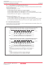
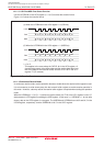
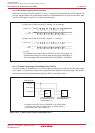
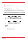
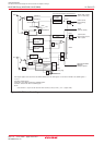
Figure 14.17 shows the typical transmit timings in UART mode. Figure 14.18 shows the typical receive
timing in UART mode.
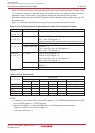
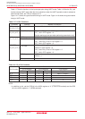
Table 14.7 I/O Pin Functions
i = 0 to 2
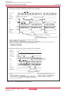
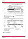
Table 14.8 P6_4 Pin Functions
TXDi
(P6_3, P6_7, P7_0)
RXDi
(P6_2, P6_6, P7_1)
CLKi
(P6_1, P6_5, P7_2)
________ ________
CTSi/RTSi
(P6_0, P6_4, P7_3)
Pin Name Function Method of Selection
Serial Data Output
Serial Data Input
I/O Port
Transfer Clock Input
_______
CTS Input
________
RTS Output
I/O Port
(Outputs “H” when performing reception only)
PD6_2 and PD6_6 bits in PD6 register = 0
PD7_1 bit in PD7 register = 0
(Can be used as an input port when performing transmission only)
CKDIR bit in UiMR register = 0
CKDIR bit in UiMR register = 1
PD6_1 and PD6_5 bits in PD6 register = 0
PD7_2 bit in PD7 register = 0
CRD bit in UiC0 register = 0
CRS bit in UiC0 register = 0
PD6_0 and PD6_4 bits in PD6 register = 0
PD7_3 bit in PD7 register = 0
CRD bit = 0
CRS bit = 1
CRD bit = 1
-: “0” or “1”
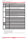
NOTE:
1.
__________ _________
In addition to this, set the CRD bit in the U0C0 register to “0” (CTS0/RTS0 enabled) and the CRS
_________
bit in the U0C0 register to “1” (RTS0 selected).
Bit set Value
Pin Function U1C0 Register UCON Register PD6 Register
CRD bit CRS bit RCSP bit CLKMD1 bit PD6_4 bit
P6_4 1 - 0 0 Input: 0, Output: 1
_________
CTS1 0 0 0 0 0
_________
RTS1 0 1 0 0 -
_________
CTS0
(1)
0010 0