


Rev.1.10 Jul 01, 2005 page 115 of 318
REJ09B0124-0110
M16C/6N Group (M16C/6NK, M16C/6NM) 12. Timers
Under development
This document is under development and its contents are subject to change.
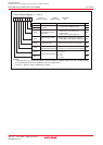
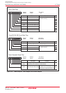
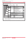
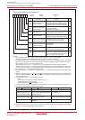
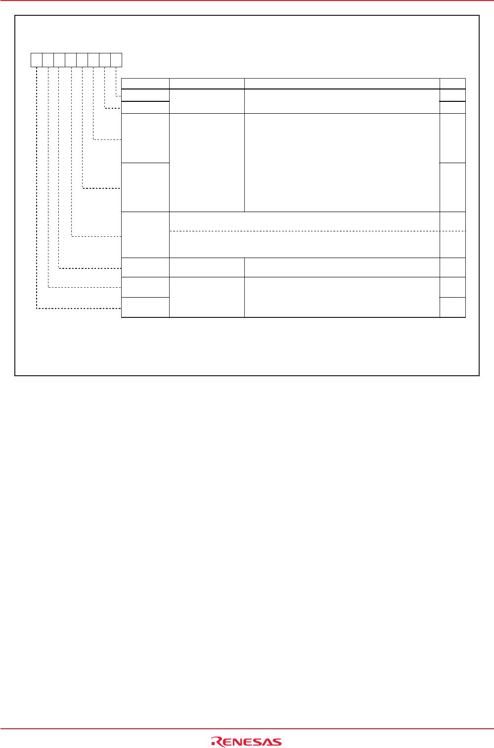
Figure 12.20
TB0MR to TB5MR Registers in Pulse Period and Pulse Width Measurement Mode
Timer Bi Mode Register (i = 0 to 5)
Bit NameBit Symbol RW
b7 b6 b5 b4 b3 b2 b1 b0
Operation Mode
Select Bit
1 0 : Pulse period / pulse width
measurement mode
b1 b0
TMOD1
TMOD0
MR0
Measurement Mode
Select Bit
MR2
MR1
MR3
TCK1
TCK0
01
0 0 : Pulse period measurement
(Measurement between a falling edge and the
next falling edge of measured pulse)
0 1 : Pulse period measurement
(Measurement between a rising edge and the next
rising edge of measured pulse)
1 0 : Pulse width measurement
(Measurement between a falling edge and the
next rising edge of measured pulse and between
a rising edge and the next falling edge)
1 1 : Do not set a value
Function
b3 b2
Count Source
Select Bit
Timer Bi Overflow
Flag
(1)
0 : Timer did not overflow
1 : Timer has overflown
0 0 : f1 or f2
0 1 : f8
1 0 : f32
1 1 : fC32
b7 b6
RW
RW
RW
RW
RW
-
RW
RW
RO
TB0MR and TB3MR registers
Set to "0" in pulse period and pulse width measurement mode
TB1MR, TB2MR, TB4MR, TB5MR registers
Nothing is assigned. When write, set to "0".
When read, its content turns out to be indeterminate.
NOTE:
1. This flag is indeterminate after reset. When the TBiS bit = 1 (start counting), the MR3 bit is set to "0" (no overflow) by writing to the
TBiMR register at the next count timing or later after the MR3 bit was set to "1" (overflow). The MR3 bit cannot be set to "1" in a
program. The TB0S to TB2S bits are assigned to the bit 5 to bit 7 in the TABSR register, and the TB3S to TB5S bits are assigned
to the bit 5 to bit 7 in the TBSR register.
After Reset
TB0MR to TB2MR 00XX0000b
TB3MR to TB5MR 00XX0000b
Address
039Bh to 039Dh
01DBh to 01DDh
Symbol