


Rev.1.10 Jul 01, 2005 page 255 of 318
REJ09B0124-0110
M16C/6N Group (M16C/6NK, M16C/6NM) 20. Flash Memory Version
Under development
This document is under development and its contents are subject to change.
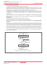
20.3.6 Data Protect Function
Each block in the flash memory has a nonvolatile lock bit. The lock bit is enabled by setting the FMR02 bit
in the FMR0 register to “0” (lock bit enabled). The lock bit allows each block to be individually protected
(locked) against program and erase. This helps prevent data from being inadvertently written to or erased
from the flash memory.
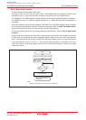
• When the lock bit status is set to “0”, the block is locked (block is protected against program and erase).
• When the lock bit status is set to “1”, the block is not locked (block can be programmed or erased).
The lock bit status is set to “0” (locked) by executing the lock bit program command and to “1” (unlocked)
by erasing the block. The lock bit status cannot be set to “1” by any commands.
The lock bit status can be read by the read lock bit status command.
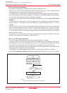
The lock bit function is disabled by setting the FMR02 bit to “1”. All blocks are unlocked. However,
individual lock bit status remains unchanged. The lock bit function is enabled by setting the FMR02 bit to
“0”. Lock bit status is retained.
If the block erase or erase all unlocked block command is executed while the FMR02 bit is set to “1”, the
target block or all blocks are erased regardless of lock bit status. The lock bit status of each block are set
to “1” after an erase operation is completed.
Refer to 20.3.5 Software Commands for details on each command.
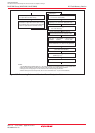
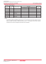
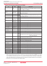
20.3.7 Status Register (SRD Register)
The status register indicates the flash memory operation state and whether or not an erase or program
operation is completed as expected. The FMR00, FMR06 and FMR07 bits in the FMR0 register indicate
status register states.
Table 20.5 shows the status register.
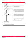
In EW0 mode, the status register can be read when the followings occur.
• Any even address in the user ROM area is read after writing the read status register command
• Any even address in the user ROM area is read from when the program, block erase, erase all unlocked
block, or lock bit program command is executed until when the read array command is executed.
20.3.7.1 Sequencer Status (SR7 and FMR00 Bits)
The sequence status indicates the flash memory operation state. It is set to “0” while the program, block
erase, erase all unlocked block, lock bit program, or read lock bit status command is being executed;
otherwise, it is set to “1”.
20.3.7.2 Erase Status (SR5 and FMR07 Bits)
Refer to 20.3.8 Full Status Check.
20.3.7.3 Program Status (SR4 and FMR06 Bits)
Refer to 20.3.8 Full Status Check.