


Rev.1.10 Jul 01, 2005 page 133 of 318
REJ09B0124-0110
M16C/6N Group (M16C/6NK, M16C/6NM) 14. Serial I/O
Under development
This document is under development and its contents are subject to change.
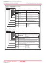
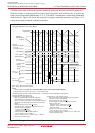
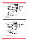
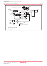
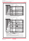
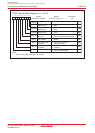
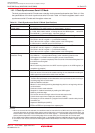
Figure 14.6 U0MR to U2MR Registers and U0C0 to U2C0 Registers
Function
UARTi Transmit/Receive Control Register 0 (i = 0 to 2)
Bit Name
Bit
Symbol
Symbol Address After Reset
U0C0 to U2C0 03A4h, 03ACh, 01FCh 00001000b
RW
CLK0
CLK1
BRG Count Source
Select Bit
Transmit Register
Empty Flag
0 0 : f1SIO or f2SIO is selected
0 1 : f8SIO is selected
1 0 : f32SIO is selected
1 1 : Do not set a value
TXEPT
0 : Data present in transmit register
(during transmission)
1 : No data present in transmit register
(transmission completed)
RW
RW
RO
Transfer Format
Select Bit
(4)
UFORM
0 : LSB first
1 : MSB first
RW
Data Output
Select Bit
(3)
NCH
0 :
TXDi/SDAi and SCLi pins are CMOS output
1 : TXDi/SDAi and SCLi pins are
N channel open-drain output
RW
CTS/RTS Function
Select Bit
(1)
CRS
Effective when CRD = 0
0 : CTS function is selected
(2)
1 : RTS function is selected
RW
CTS/RTS Disable Bit
CRD
0 : CTS/RTS function enabled
1 : CTS/RTS function disabled
(P6_0, P6_4, P7_3 can be used as I/O ports)
RW
CLK Polarity
Select Bit
CKPOL
0 : Transmit data is output at falling edge
of transfer clock and receive data is
input at rising edge
1 : Transmit data is output at rising edge
of transfer clock and receive data is
input at falling edge
RW
b1 b0
b7 b6 b5 b4 b3 b2 b1 b0
NOTES:
1.CTS1/RTS1 can be used when the CLKMD1 bit in the UCON register = 0 (only CLK1 output) and the
RCSP bit in the UCON register = 0 (CTS0/RTS0 not separated).
2. Set the corresponding port direction bit for each CTSi pin to "0" (input mode)
3. SCL2(P7_1) is N channel open-drain output. The NCH bit in the U2C0 register is N channel open-drain
output regardless of the NCH bit.
4.The UFORM bit is enabled when the SMD2 to SMD0 bits in the UiMR register are set to "001b" (clock
synchronous serial I/O mode), or "101b" (UART mode, 8-bit transfer data).
Set this bit to "1" when the SMD2 to SMD0 bits are set to "010b" (I
2
C mode), and to "0" when the SMD2
to SMD0 bits are set to "100b" (UART mode, 7-bit transfer data) or "110b" (UART mode, 9-bit transfer data).
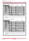
b7 b6 b5 b4 b3 b2 b1 b0
Function
UARTi Transmit/Receive Mode Register (i = 0 to 2)
Bit Name
Bit
Symbol
Symbol Address After Reset
U0MR to U2MR 03A0h, 03A8h, 01F8h 00h
RW
SMD0
SMD1
SMD2
Serial I/O Mode
Select Bit
(1)
CKDIR
Internal/External Clock
Select Bit
Stop Bit Length
Select Bit
0 0 0
: Serial I/O disabled
0 0 1
: Clock synchronous serial I/O mode
0 1 0
:
I
2
C mode
(2)
1 0 0
: UART mode transfer data 7-bit long
1 0 1
: UART mode transfer data 8-bit long
1 1 0
: UART mode transfer data 9-bit long
Do not set a value except above
0 : Internal clock
1 : External clock
(3)
STPS
0 : 1 stop bit
1 : 2 stop bits
NOTES:
1. To receive data, set the corresponding port direction bit for each RXDi pin to "0" (input mode).
2. Set the corresponding port direction bit for SCL and SDA pins to "0" (input mode).
3. Set the corresponding port direction bit for each CLKi pin to "0" (input mode).
RW
RW
RW
RW
RW
TXD, RXD I/O Polarity
Reverse Bit
IOPOL
0 : No reverse
1 : Reverse
RW
Parity Enable Bit
PRYE
0 : Parity disabled
1 : Parity enabled
RW
Odd/Even Parity
Select Bit
PRY
Effective when the PRYE bit = 1
0 : Odd parity
1 : Even parity
RW
b2 b1 b0