


Rev.1.10 Jul 01, 2005 page 112 of 318
REJ09B0124-0110
M16C/6N Group (M16C/6NK, M16C/6NM) 12. Timers
Under development
This document is under development and its contents are subject to change.
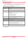
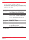
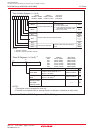
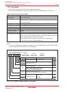
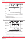
Item Specification
Count Source f1, f2, f8, f32, fC32
Count Operation • Down-count
• When the timer underflows, it reloads the reload register contents and
continues counting
Divide Ratio 1/(n+1) n: set value of the TBi register 0000h to FFFFh
Count Start Condition Set the TBiS bit
(1)
to “1” (start counting)
Count Stop Condition Set the TBiS bit to “0” (stop counting)
Interrupt Request Generation Timing
Timer underflow
TBiIN Pin Function I/O port
Read from Timer Count value can be read by reading the TBi register
Write to Timer • When not counting and until the 1st count source is input after counting start
Value written to the TBi register is written to both reload register and counter
• When counting (after 1st count source input)
Value written to the TBi register is written to only reload register
(Transferred to counter when reloaded next)
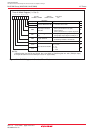
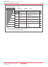
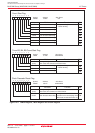
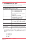
12.2.1 Timer Mode
In timer mode, the timer counts a count source generated internally.
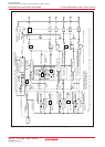
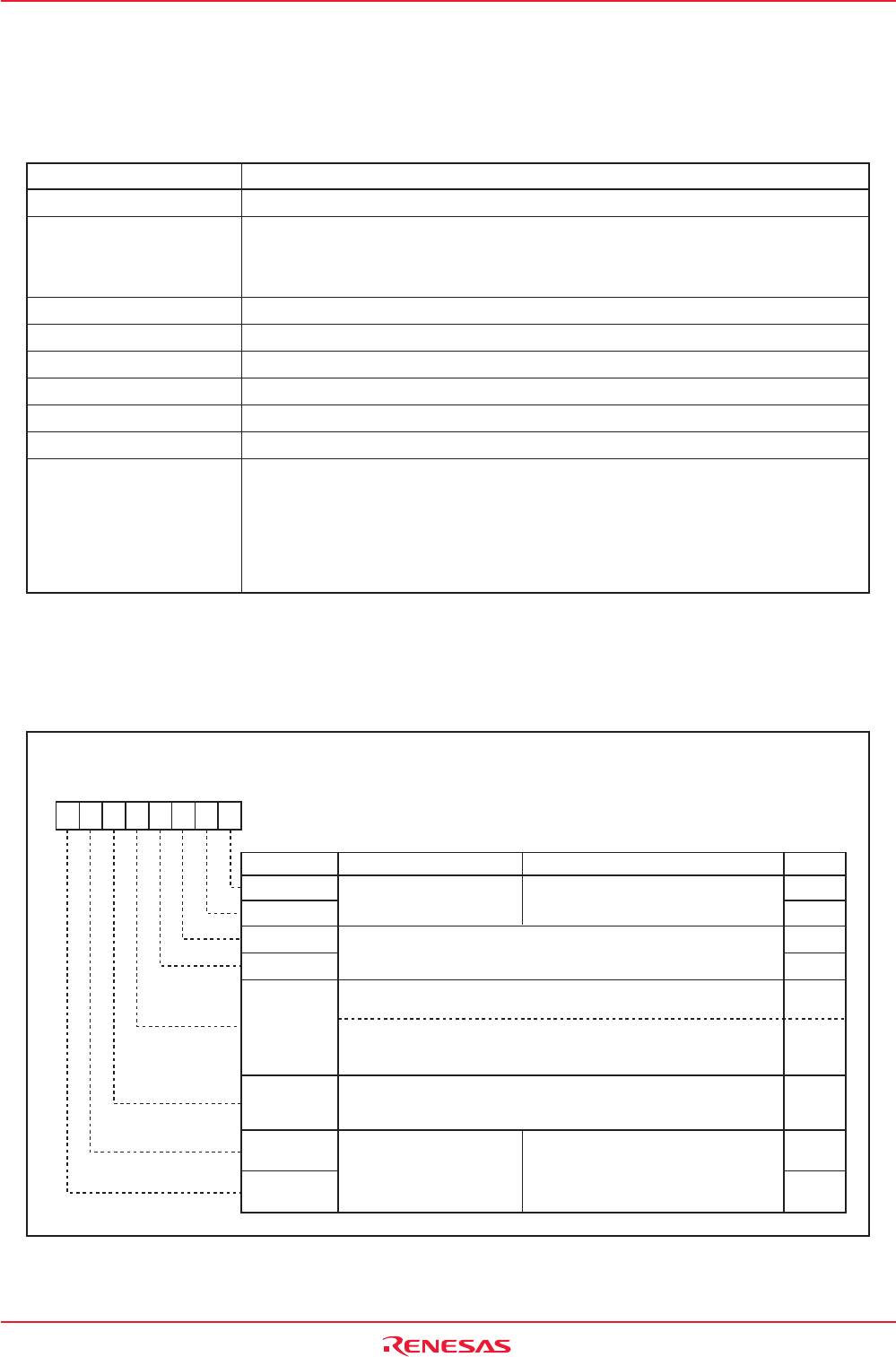
Table 12.6 lists specifications in timer mode. Figure 12.18 shows TBiMR register in timer mode.
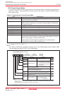
Table 12.6 Specifications in Timer Mode
Symbol After Reset
TB0MR to TB2MR 00XX0000b
TB3MR to TB5MR 00XX0000b
Bit Name Function
Bit Symbol
RW
b7 b6 b5 b4 b3 b2 b1 b0
Operation Mode Select Bit
0 0 : Timer mode
b1 b0
TMOD1
TMOD0
MR0
Has no effect in timer mode
Can be set to "0" or "1"
MR2
MR1
MR3
0 0 : f1 or f2
0 1 : f8
1 0 : f32
1 1 : fC32
TCK1
TCK0
Count Source Select Bit
00
TB0MR, TB3MR registers
Set to "0" in timer mode
b7 b6
RW
RW
RW
RW
RW
-
RW
RW
RO
TB1MR, TB2MR, TB4MR, TB5MR registers
Nothing is assigned. When write, set to "0".
When read, its content is indeterminate.
When write in timer mode, set to "0".
When read in timer mode, its content is indeterminate.
Address
039Bh to 039Dh
01DBh to 01DDh
Timer Bi Mode Register (i = 0 to 5)
i = 0 to 5
NOTE:
1. The TB0S to TB2S bits are assigned to the bit 5 to bit 7 in the TABSR register, and the TB3S to TB5S
bits are assigned to the bit 5 to bit 7 in the TBSR register.
Figure 12.18 TB0MR to TB5MR Registers in Timer Mode