


Rev.1.10 Jul 01, 2005 page 260 of 318
REJ09B0124-0110
M16C/6N Group (M16C/6NK, M16C/6NM) 20. Flash Memory Version
Under development
This document is under development and its contents are subject to change.
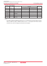
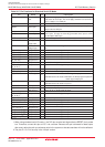
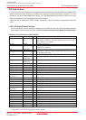
Table 20.7 Pin Functions for Standard Serial I/O Mode
NOTES:
1.
___________
When using standard serial I/O mode 1, the TXD pin must be held high while the RESET pin is pulled
low. Therefore, connect this pin to VCC1 via a resistor. Because this pin is directed for data output
after reset, adjust the pull-up resistance value in the system so that data transfers will not be affected.
2. The pins P11 to P14 are only in the 128-pin version.
Apply the voltage guaranteed for Program and Erase to VCC1 pin
and VCC2 to VCC2 pin. The VCC apply condition is that VCC2 =
VCC1. Apply 0 V to VSS pin.
Connect to VCC1 pin.
____________
Reset input pin. While RESET pin is "L" level, input 20 cycles or
longer clock to XIN pin.
Connect a ceramic resonator or crystal oscillator between XIN and
XOUT pins. To input an externally generated clock, input it to XIN
pin and open XOUT pin.
Connect this pin to VCC1 or VSS.
Connect AVCC to VCC1 and AVSS to VSS, respectively.
Enter the reference voltage for A/D and D/A converters from this
pin.
Input “H” or “L” level signal or open.
Input “H” or “L” level signal or open.
Input “H” or “L” level signal or open.
Input “H” or “L” level signal or open.
Input “H” or “L” level signal or open.
Input “H” level signal.
Input “H” or “L” level signal or open.
Input “L” level signal.
Input “H” or “L” level signal or open.
Standard serial I/O mode 1: BUSY signal output pin
Standard serial I/O mode 2: Monitors the boot program operation
check signal output pin.
Standard serial I/O mode 1: Serial clock input pin.
Standard serial I/O mode 2: Input “L”.
Serial data input pin
Serial data output pin
(1)
Input “H” or “L” level signal or open.
Input “H” or “L” level signal or open.
Connect this pin to VCC1.
Input “H” or “L” level signal or open.
Input “H” or “L” level signal or connect to a CAN transceiver.
Input “H” level signal, open or connect to a CAN transceiver.
Input “H” or “L” level signal or open.
Input “H” or “L” level signal or open.
Input “H” or “L” level signal or open.
Input “H” or “L” level signal or open.
Input “H” or “L” level signal or open.
VCC1, VCC2, VSS
CNVSS
_____________
RESET
XIN
XOUT
BYTE
AVCC, AVSS
VREF
P0_0 to P0_7
P1_0 to P1_7
P2_0 to P2_7
P3_0 to P3_7
P4_0 to P4_7
P5_0
P5_1 to P5_4,
P5_6, P5_7
P5_5
P6_0 to P6_3
_________
P6_4/RTS1
P6_5/CLK1
P6_6/RXD1
P6_7/TXD1
P7_0 to P7_7
P8_0 to P8_4,
P8_6, P8_7
_______
P8_5/NMI
P9_0 to P9_4, P9_7
P9_5/CRX0
P9_6/CTX0
P10_0 to P10_7
P11_0 to P11_7
(2)
P12_0 to P12_7
(2)
P13_0 to P13_7
(2)
P14_0, P14_1
(2)
I
I
I
O
I
I
I
I
I
I
I
I
I
I
I
O
I
I
O
I
I
I
I
I
O
I
I
I
I
I
Pin Name I/O
Description
Power supply
input
CNVSS
Reset input
Clock input
Clock output
BYTE
Analog power
supply input
Reference
voltage input
Input port P0
Input port P1
Input port P2
Input port P3
Input port P4
_____
CE input
Input port P5
________
EPM input
Input port P6
BUSY output
SCLK input
RXD input
TXD output
Input port P7
Input port P8
________
NMI input
Input port P9
CRX input
CTX output
Input port P10
Input port P11
Input port P12
Input port P13
Input port P14