


Rev.1.10 Jul 01, 2005 page 178 of 318
REJ09B0124-0110
M16C/6N Group (M16C/6NK, M16C/6NM) 14. Serial I/O
Under development
This document is under development and its contents are subject to change.
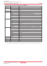
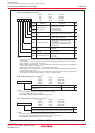
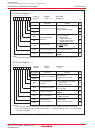
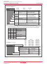
Item Specification
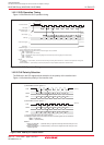
Transfer Data Format Transfer data length: 8 bits
Transfer clock • SMi6 bit in SiC register = 1 (internal clock) : fj/ 2(n+1)
fj = f1SIO, f8SIO, f32SIO. n = Setting value of SiBRG register 00h to FFh
• SMi6 bit = 0 (external clock) : Input from CLKi pin
(1)
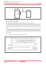
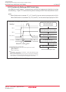
Transmission/Reception Before transmission/reception can start, the following requirements must be met
Start Condition Write transmit data to the SiTRR register
(2) (3)
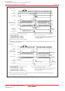
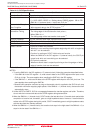
Interrupt Request • When SMi4 bit in SiC register = 0
Generation Timing The rising edge of the last transfer clock pulse
(4)
• When SMi4 bit = 1
The falling edge of the last transfer clock pulse
(4)
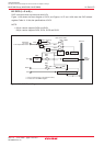
CLKi Pin Function I/O port, transfer clock input, transfer clock output
SOUTi Pin Function I/O port, transmit data output, high-impedance
SINi Pin Function I/O port, receive data input
Select Function • LSB first or MSB first selection
Whether to start sending/receiving data beginning with bit 0 or beginning
with bit 7 can be selected
• Function for setting an SOUTi initial value set function
When the SMi6 bit in the SiC register = 0 (external clock), the SOUTi pin
output level while not transmitting can be selected.
• CLK polarity selection
Whether transmit data is output/input timing at the rising edge or falling
edge of transfer clock can be selected.
Table 14.19 SI/Oi Specifications
i = 3 to 6 (5 and 6 are only in the 128-pin version.)
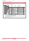
NOTES:
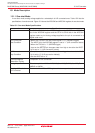
1.To set the SMi6 bit in the SiC register to “0” (external clock), follow the procedure described below.
• If the SMi4 bit in the SiC register = 0, write transmit data to the SiTRR register while input on the
CLKi pin is high. The same applies when rewriting the SMi7 bit in the SiC register.
• If the SMi4 bit = 1, write transmit data to the SiTRR register while input on the CLKi pin is low. The
same applies when rewriting the SMi7 bit.
• Because shift operation continues as long as the transfer clock is supplied to the SI/Oi circuit, stop
the transfer clock after supplying eight pulses. If the SMi6 bit = 1 (internal clock), the transfer clock
automatically stops.
2.Unlike UART0 to UART2, SI/Oi is not separated between the transfer register and buffer. Therefore,
do not write the next transmit data to the SiTRR register during transmission.
3. When the SMi6 bit = 1 (internal clock), SOUTi retains the last data for a 1/2 transfer clock period after
completion of transfer and, thereafter, goes to a high-impedance state. However, if transmit data is
written to the SiTRR register during this period, SOUTi immediately goes to a high-impedance state,
with the data hold time thereby reduced.
4.When the SMi6 bit = 1 (internal clock), the transfer clock stops in the high state if the SMi4 bit = 0, or
stops in the low state if the SMi4 bit = 1.