


Rev.1.10 Jul 01, 2005 page 135 of 318
REJ09B0124-0110
M16C/6N Group (M16C/6NK, M16C/6NM) 14. Serial I/O
Under development
This document is under development and its contents are subject to change.
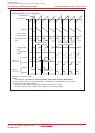
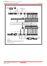
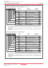
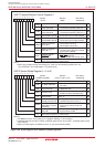
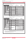
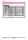
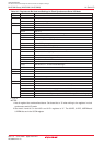
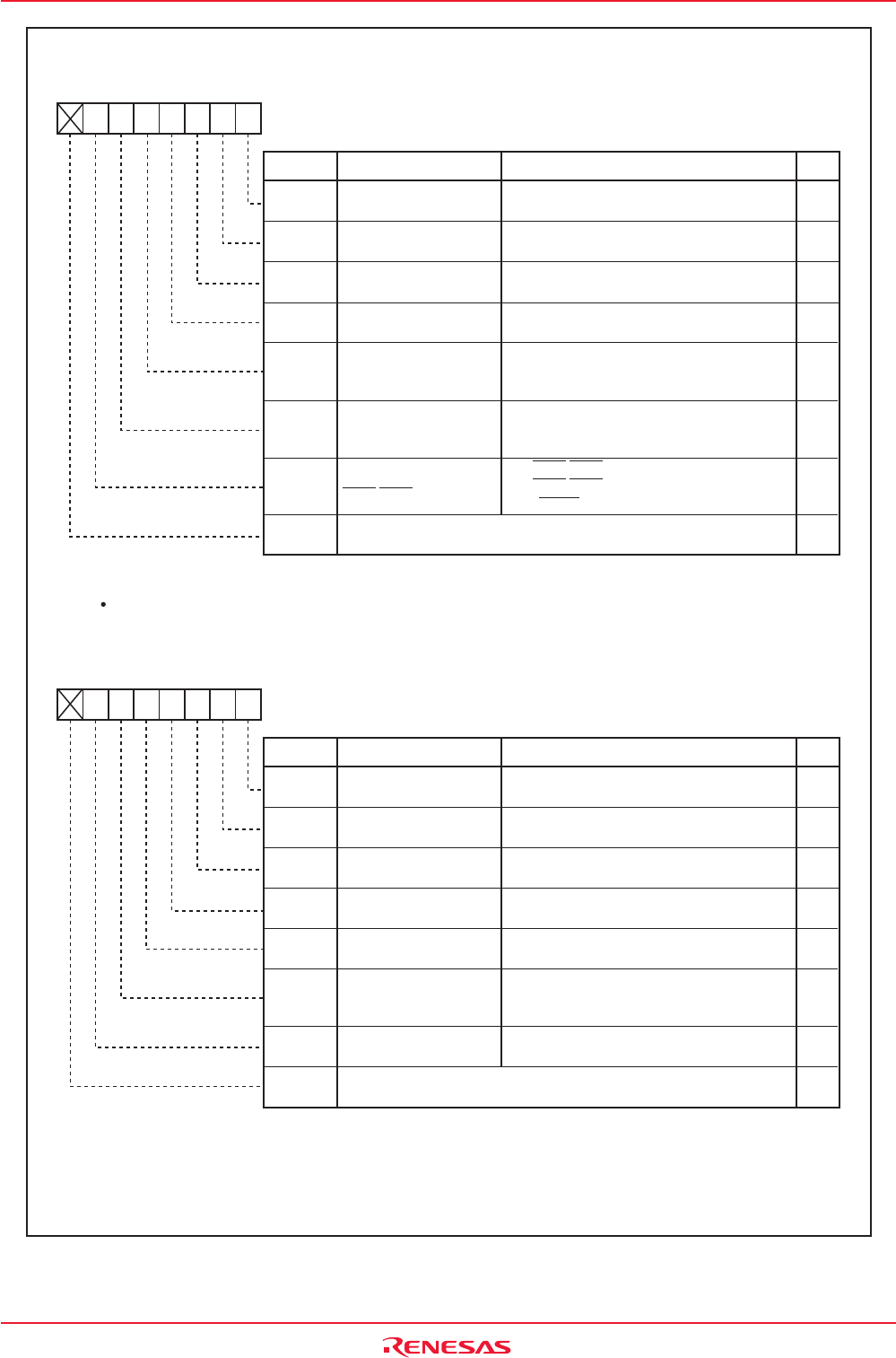
Figure 14.8 UCON Register and U0SMR to U2SMR Registers
b7 b6 b5 b4 b3 b2 b1 b0
Function
UART Transmit/Receive Control Register 2
Bit Name
Bit
Symbol
Symbol Address After Reset
UCON 03B0h X0000000b
RW
U0IRS
U1IRS
U0RRM
UART1 Transmit Interrupt
Cause Select Bit
UART0 Continuous
Receive Mode Enable Bit
UART0 Transmit Interrupt
Cause Select Bit
U1RRM
UART1 Continuous
Receive Mode Enable Bit
0 : Transmit buffer empty (Tl bit = 1)
1 :
Transmission completed (TXEPT bit = 1)
0 : Transmit buffer empty (Tl bit = 1)
1 :
Transmission completed (TXEPT bit = 1)
0 : Continuous receive mode disabled
1 : Continuous receive mode enabled
0 : Continuous receive mode disabled
1 : Continuous receive mode enabled
RW
RW
RW
RW
Nothing is assigned. When write, set to "0".
When read, its content is indeterminate.
-
Separate UART0
CTS/RTS Bit
RCSP
0 : CTS/RTS shared pin
1 : CTS/RTS separated
(CTS0 supplied from the P6_4 pin)
RW
UART1 CLK/CLKS
Select Bit 1
(1)
CLKMD1
0 : CLK output is only CLK1
1 : Transfer clock output from multiple
pins function selected
RW
UART1 CLK/CLKS
Select Bit 0
CLKMD0
Effective when the CLKMD1 bit = 1
0 : Clock output from CLK1
1 : Clock output from CLKS1
RW
NOTE:
1. When using multiple transfer clock output pins, make sure the following conditions are met:
The CKDIR bit in the U1MR register = 0 (internal clock)
-
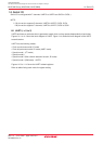
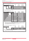
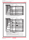
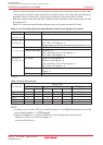
(b7)
b7 b6 b5 b4 b3 b2 b1 b0
Function
UARTi Special Mode Register (i = 0 to 2)
Bit Name
Bit
Symbol
Symbol Address After Reset
U0SMR to U2SMR 01EFh, 01F3h, 01F7h X0000000b
RW
IICM
ABC
BBS
Arbitration Lost Detecting
Flag Control Bit
Bus Busy Flag
I
2
C Mode Select Bit
-
(b3)
Reserved Bit
0 : Other than I
2
C mode
1 : I
2
C mode
0 : Update per bit
1 : Update per byte
0 : STOP condition detected
1 : START condition detected (busy)
Set to "0"
RW
RW
RW
(1)
RW
Nothing is assigned. When write, set to "0".
When read, its content is indeterminate.
-
(b7)
-
Transmit Start Condition
Select Bit
SSS
0 : Not synchronized to RXDi
1 : Synchronized to RXDi
(3)
RW
Auto Clear Function
Select Bit of Transmit
Enable Bit
ACSE
0 : No auto clear function
1 : Auto clear at occurrence of bus
collision
RW
Bus Collision Detect
Sampling Clock Select Bit
ABSCS
0 : Rising edge of transfer clock
1 : Underflow signal of timer Aj
(2)
RW
NOTES:
1. The BBS bit is set to "0" by writing "0" in a program. (Writing "1" has no effect.).
2. Underflow signal of timer A3 in UART0, underflow signal of timer A4 in UART1, underflow signal of timer
A0 in UART2.
3. When a transfer begins, the SSS bit is set to "0" (not synchronized to RXDi).
0