


Rev.1.10 Jul 01, 2005 page 144 of 318
REJ09B0124-0110
M16C/6N Group (M16C/6NK, M16C/6NM) 14. Serial I/O
Under development
This document is under development and its contents are subject to change.
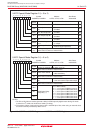
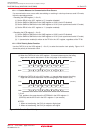
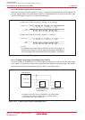
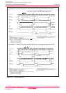
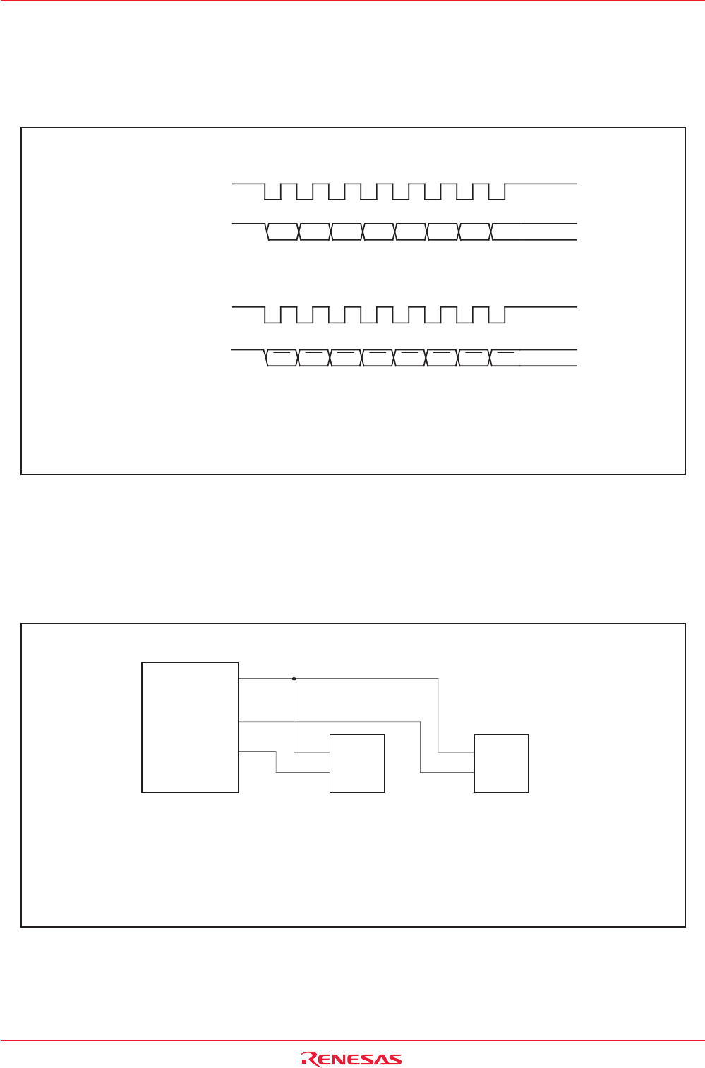
14.1.1.5 Serial Data Logic Switching Function
When the UiLCH bit in the UiC1 register (i = 0 to 2) = 1 (reverse), the data written to the UiTB register has
its logic reversed before being transmitted. Similarly, the received data has its logic reversed when read
from the UiRB register. Figure 14.14 shows serial data logic.
Figure
14.14
Serial Data Logic Switching
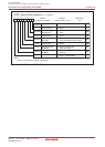
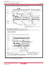
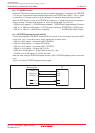
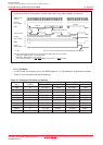
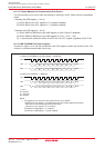
14.1.1.6 Transfer Clock Output From Multiple Pins (UART1)
Use the CLKMD1 to CLKMD0 bits in the UCON register to select one of the two transfer clock output
pins. Figure 14.15 shows the transfer clock output from the multiple pins function usage. This function
can be used when the selected transfer clock for UART1 is an internal clock.
Figure 14.15 Transfer Clock Output From Multiple Pins
D0 D1 D2 D3 D4 D5 D6 D7
Transfer clock
TXDi
(no reverse)
"H"
"L"
"H"
"L"
TXDi
(reverse)
D0 D1 D2 D3 D4 D5 D6 D7
"H"
"L"
(1) When the UiLCH bit in the UiC1 register = 0 (no reverse)
Transfer clock
"H"
"L"
(2) When the UiLCH bit in the UiC1 register = 1 (reverse)
* This applies to the case where the CKPOL bit in the UiC0 register = 0
(transmit data output at the falling edge and the receive data taken in
at the rising edge of the transfer clock) and the UFORM bit = 0 (LSB first).
i = 0 to 2
Microcomputer
IN
CLK
IN
CLK
* This applies to the case where the CKDIR bit in the U1MR register
= 0 (internal clock) and the CLKMD1 bit in the UCON register = 1
(transfer clock output from multiple pins).
Transfer enabled when
the CLKMD0 bit in the
UCON register = 0
Transfer enabled when
the CLKMD0 bit = 1
TXD1(P6_7)
CLKS1(P6_4)
CLK1(P6_5)