


Rev.1.10 Jul 01, 2005 page 199 of 318
REJ09B0124-0110
M16C/6N Group (M16C/6NK, M16C/6NM) 16. D/A Converter
Under development
This document is under development and its contents are subject to change.
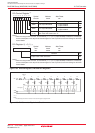
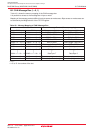
Figure 16.2 DACON Register, DA0 and DA1 Registers
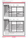
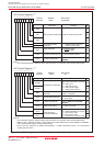
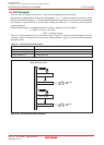
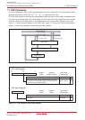
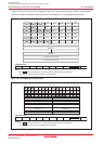
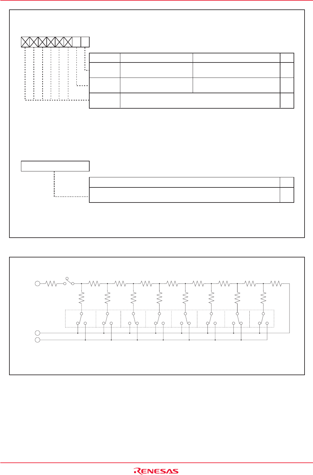
Figure 16.3 D/A Converter Equivalent Circuit
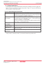
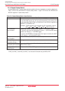
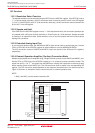
D/A Control Register
(1)
Symbol Address After Reset
Symbol Address After Reset
DACON 03DCh
03D8h
03DAh
00h
b7 b6 b5 b4 b3 b2 b1 b0
D/A0 Output Enable Bit
Bit Symbol Bit Name Function
RW
D/A1 Output Enable Bit
DA0
DA1
00h
00h
b7 b0
Function
Output value of D/A conversion
RW
RW
-
RW
RW
DA0E
DA1E
-
(b7-b2)
0 : Output disabled
1 : Output enabled
0 : Output disabled
1 : Output enabled
Nothing is assigned. When write, set to "0".
When read, their contents are "0".
NOTE:
1. When not using the D/A converter, set the DAiE bit (i = 0, 1) to "0" (output disabled) to reduce the unnecessary
current consumption in the chip and set the DAi register to "00h" to prevent current from flowing into the R-2R
resistor ladder.
NOTE:
1. When not using the D/A converter, set the DAiE bit (i = 0, 1) to "0" (output disabled) to reduce the unnecessary
current consumption in the chip and set the DAi register to "00h" to prevent current from flowing into the R-2R
resistor ladder.
D/A Register i (i = 0, 1)
(1)
2R
R
2R
R
2R
R
2R
R
2R
R
2R
R
2R
R
2R
2R
DAiE bit
"1""0"
MSB LSB
DAi register
r
i = 0, 1
NOTE:
1. The above diagram shows an instance in which the DAi register is assigned "2Ah".
"1"
"0"
VREF
AVSS
DAi