


Rev.1.10 Jul 01, 2005 page 297 of 318
REJ09B0124-0110
M16C/6N Group (M16C/6NK, M16C/6NM) 22. Usage Precaution
Under development
This document is under development and its contents are subject to change.
22.11 Serial I/O
22.11.1 Clock Synchronous Serial I/O Mode
22.11.1.1 Transmission/reception
_______ ________
With an external clock selected, and choosing the RTS function, the output level of the RTSi pin goes to
“L” when the data-receivable status becomes ready, which informs the transmission side that the recep-
________ ________
tion has become ready. The output level of the RTSi pin goes to “H” when reception starts. So if the RTSi
________
pin is connected to the CTSi pin on the transmission side, the circuit can transmission and reception
_______
data with consistent timing. With the internal clock, the RTS function has no effect.
_______
If a low-level signal is applied to the NMI pin when the IVPCR1 bit in the TB2SC register = 1 (three-
_______ _________
phase output forcible cutoff by input on NMI pin enabled), the RTS2 and CLK2 pins go to a high-imped-
ance state.
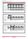
22.11.1.2 Transmission
When an external clock is selected, the conditions must be met while if the CKPOL bit in the UiC0
register = 0 (transmit data output at the falling edge and the receive data taken in at the rising edge of the
transfer clock), the external clock is in the high state; if the CKPOL bit = 1 (transmit data output at the
rising edge and the receive data taken in at the falling edge of the transfer clock), the external clock is in
the low state.
• The TE bit in the UiC1 register = 1 (transmission enabled)
• The TI bit in the UiC1 register = 0 (data present in UiTB register)
_______ ________
• If CTS function is selected, input on the CTSi pin = L
22.11.1.3 Reception
In operating the clock synchronous serial I/O, operating a transmitter generates a shift clock. Fix settings
for transmission even when using the device only for reception. Dummy data is output to the outside
from the TXDi (i = 0 to 2) pin when receiving data.
When an internal clock is selected, set the TE bit in the UiC1 register to “1” (transmission enabled) and
write dummy data to the UiTB register, and the shift clock will thereby be generated. When an external
clock is selected, set the TE bit to “1” and write dummy data to the UiTB register, and the shift clock will
be generated when the external clock is fed to the CLKi input pin.
When successively receiving data, if all bits of the next receive data are prepared in the UARTi receive
register while the RI bit in the UiC1 register = 1 (data present in the UiRB register), an overrun error
occurs and the OER bit in the UiRB register is set to “1” (overrun error occurred). In this case, because
the content of the UiRB register is indeterminate, a corrective measure must be taken by programs on
the transmit and receive sides so that the valid data before the overrun error occurred will be retransmitted.
Note that when an overrun error occurred, the IR bit in the SiRIC register does not change state.
To receive data in succession, set dummy data in the lower-order byte of the UiTB register every time
reception is made.
When an external clock is selected, the conditions must be met while if the CKPOL bit = 0, the external
clock is in the high state; if the CKPOL bit = 1, the external clock is in the low state.
• The RE bit in the UiC1 register = 1 (reception enabled)
• The TE bit in the UiC1 register = 1 (transmission enabled)
• The TI bit in the UiC1 register = 0 (data present in the UiTB register)