


Rev.1.10 Jul 01, 2005 page 173 of 318
REJ09B0124-0110
M16C/6N Group (M16C/6NK, M16C/6NM) 14. Serial I/O
Under development
This document is under development and its contents are subject to change.
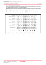
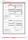
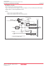
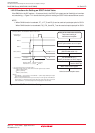
Figure 14.33 shows the example of connecting the SIM interface. Connect TXD2 and RXD2 and apply pull-up.
Figure 14.33 SIM Interface Connection
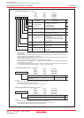
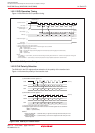
14.1.6.1 Parity Error Signal Output
The parity error signal is enabled by setting the U2ERE bit in the U2C1 register to “1”.
The parity error signal is output when a parity error is detected while receiving data. This is achieved by
pulling the TXD2 output low with the timing shown in Figure 14.32. If the R2RB register is read while
outputting a parity error signal, the PER bit is set to “0” and at the same time the TXD2 output is returned
high.
When transmitting, a transmission-finished interrupt request is generated at the falling edge of the transfer
clock pulse that immediately follows the stop bit. Therefore, whether a parity signal has been returned
can be determined by reading the port that shares the RXD2 pin in a transmission-finished interrupt
service routine.
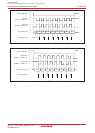
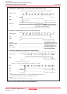
Figure 14.34 shows the output timing of the parity error signal
Figure 14.34 Parity Error Signal Output Timing
Microcomputer
SIM card
TXD2
RXD2
D0 D1 D2 D3 D4 D5 D6 D7 P SPST
(NOTE 1)
Transfer
clock
RXD2
TXD2
"H"
"L"
"H"
"L"
"H"
"L"
"1"
"0"
This timing diagram applies to the case where the direct format is
implemented.
NOTE:
1: The output of microcomputer is in the high-impedance state (pulled up externally).
ST: Start bit
P: Even Parity
SP: Stop bit
RI bit in
U2C1 register