


Rev.1.10 Jul 01, 2005 page 235 of 318
REJ09B0124-0110
M16C/6N Group (M16C/6NK, M16C/6NM) 19. Programmable I/O Ports
Under development
This document is under development and its contents are subject to change.
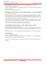
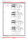
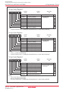
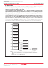
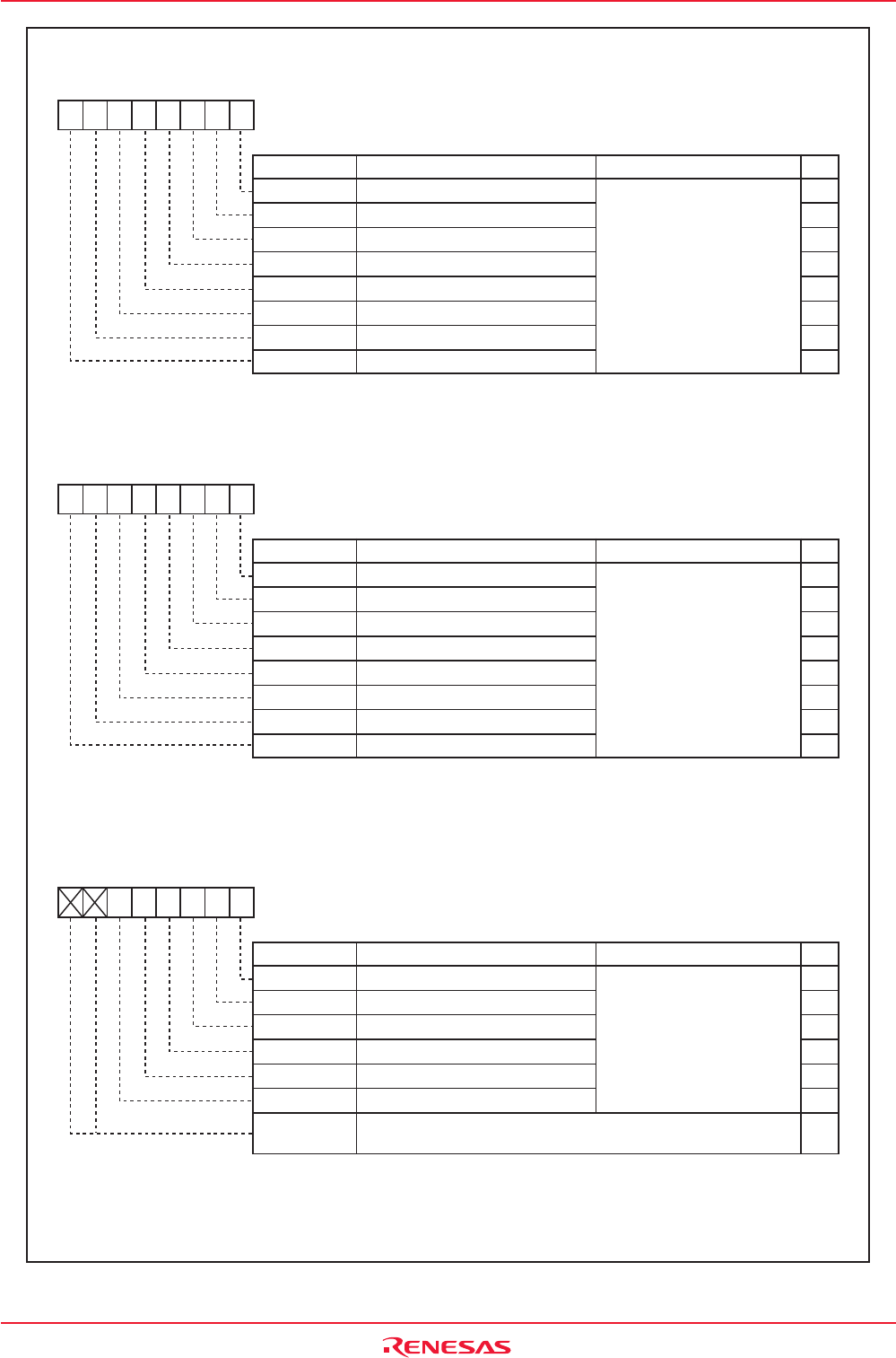
Pull-up Control Register 0
Bit NameBit Symbol RW
b7 b6 b5 b4 b3 b2 b1 b0
PUR0
03FCh
00h
Symbol Address After Reset
NOTE:
1. The pin for which this bit is "1" (pulled high) and the direction bit is "0" (input mode) is pulled high.
PU00
PU01
PU02
PU03
PU04
PU05
PU06
PU07
P0_0 to P0_3 Pull-Up
P0_4 to P0_7 Pull-Up
P1_0 to P1_3 Pull-Up
P1_4 to P1_7 Pull-Up
P2_0 to P2_3 Pull-Up
P2_4 to P2_7 Pull-Up
P3_0 to P3_3 Pull-Up
P3_4 to P3_7 Pull-Up
0 : Not pulled high
1 : Pulled high
(1)
RW
RW
RW
RW
RW
RW
RW
RW
Function
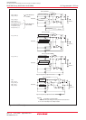
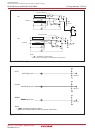
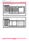
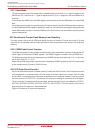
Pull-up Control Register 1
Bit NameBit Symbol RW
b7 b6 b5 b4 b3 b2 b1 b0
PUR1
03FDh
00h
Symbol Address After Reset
NOTES:
1. The P7_1 pin does not have pull-up.
2. The pin for which this bit is "1" (pulled high) and the direction bit is "0" (input mode) is pulled high.
PU10
PU11
PU12
PU13
PU14
PU15
PU16
PU17
P4_0 to P4_3 Pull-Up
P4_4 to P4_7 Pull-Up
P5_0 to P5_3 Pull-Up
P5_4 to P5_7 Pull-Up
P6_0 to P6_3 Pull-Up
P6_4 to P6_7 Pull-Up
P7_0, P7_2 and P7_3 Pull-Up
(1)
P7_4 to P7_7 Pull-Up
0 : Not pulled high
1 : Pulled high
(2)
RW
RW
RW
RW
RW
RW
RW
RW
Function
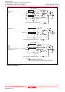
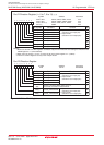
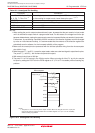
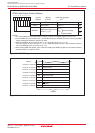
Pull-up Control Register 2
Bit NameBit Symbol RW
b7 b6 b5 b4 b3 b2 b1 b0
PUR2
03FEh
00h
Symbol Address After Reset
NOTES:
1. The P8_5 pin does not have pull-up.
2. The P9_1 pin does not have pull-up.
3. The pin for which this bit is "1" (pulled high) and the direction bit is "0" (input mode) is pulled high.
PU20
PU21
PU22
PU23
PU24
PU25
-
(b7-b6)
P8_0 to P8_3 Pull-Up
P8_4, P8_6 and P8_7 Pull-Up
(1)
P9_0, P9_2 and P9_3 Pull-Up
(2)
P9_4 to P9_7 Pull-Up
P10_0 to P10_3 Pull-Up
P10_4 to P10_7 Pull-Up
0 : Not pulled high
1 : Pulled high
(3)
RW
RW
RW
RW
RW
RW
-
Function
Nothing is assigned. When write, set to "0".
When read, their contents are "0".
Figure19.9 PUR0, PUR1 and PUR2 Registers