


Rev.1.10 Jul 01, 2005 page 4 of 318
REJ09B0124-0110
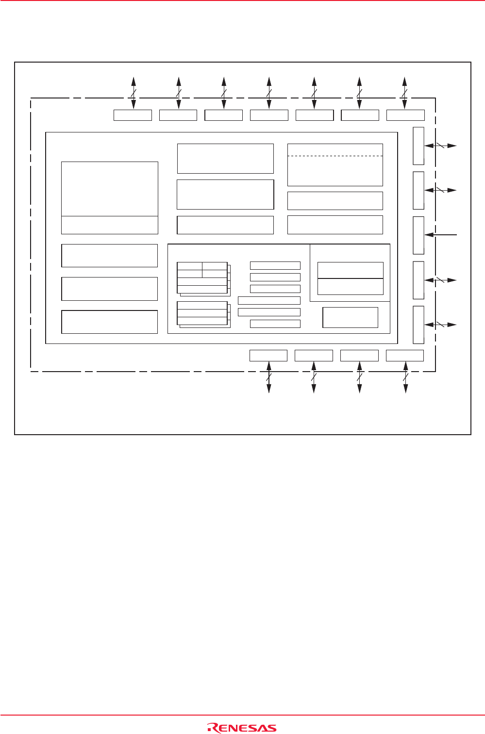
M16C/6N Group (M16C/6NK, M16C/6NM) 1. Overview
Under development
This document is under development and its contents are subject to change.
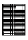
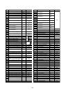
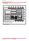
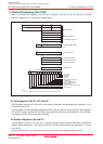
1.3 Block Diagram
Figure 1.1 shows a block diagram of M16C/6N Group (M16C/6NK, M16C/6NM).
Figure 1.1 Block Diagram
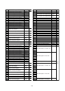
NOTES:
1: ROM size depends on microcomputer type.
2: RAM size depends on microcomputer type.
3: Ports P11 to P14 are only in the 128-pin version.
4: 8 bits ✕ 2 channels in the 100-pin version.
Port P11
8
(3)
2
Port P14
(3)
8
Port P12
(3)
8
Port P13
(3)
Timer (16 bits)
Output (timer A): 5
Input (timer B): 6
Three-phase motor
control circuit
Internal peripheral functions
Watchdog timer
(15 bits)
A/D converter
(10 bits ✕ 8 channels
Expandable up to 26 channels)
UART or
Clock synchronous serial I/O
(3 channels)
System clock generating circuit
XIN-XOUT
XCIN-XCOUT
PLL frequency synthesizer
On-chip oscillator
Port P0
8
Port P1
8
Port P2
8 8 8 8
Port P6
8
8
7
8
8
Port P10
Port P9
Port P8_5
Port P8
Port P7
Port P5Port P4Port P3
CRC arithmetic circuit (CCITT)
(Polynomial: X
16
+X
12
+X
5
+1)
Clock synchronous serial I/O
(8 bits ✕ 4 channels)
(4)
CAN module
(2 channels)
DMAC
(2 channels)
D/A converter
(8 bits ✕ 2 channels)
MemoryM16C/60 series CPU core
R0H R0L
R1H R1L
R2
R3
A0
A1
FB
Multiplier
INTB
PC
USP
ISP
SB
FLG
ROM
(1)
RAM
(2)