


Rev.1.10 Jul 01, 2005 page 74 of 318
REJ09B0124-0110
M16C/6N Group (M16C/6NK, M16C/6NM) 9. Interrupt
Under development
This document is under development and its contents are subject to change.
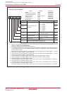
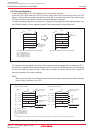
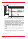
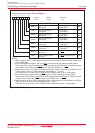
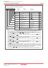
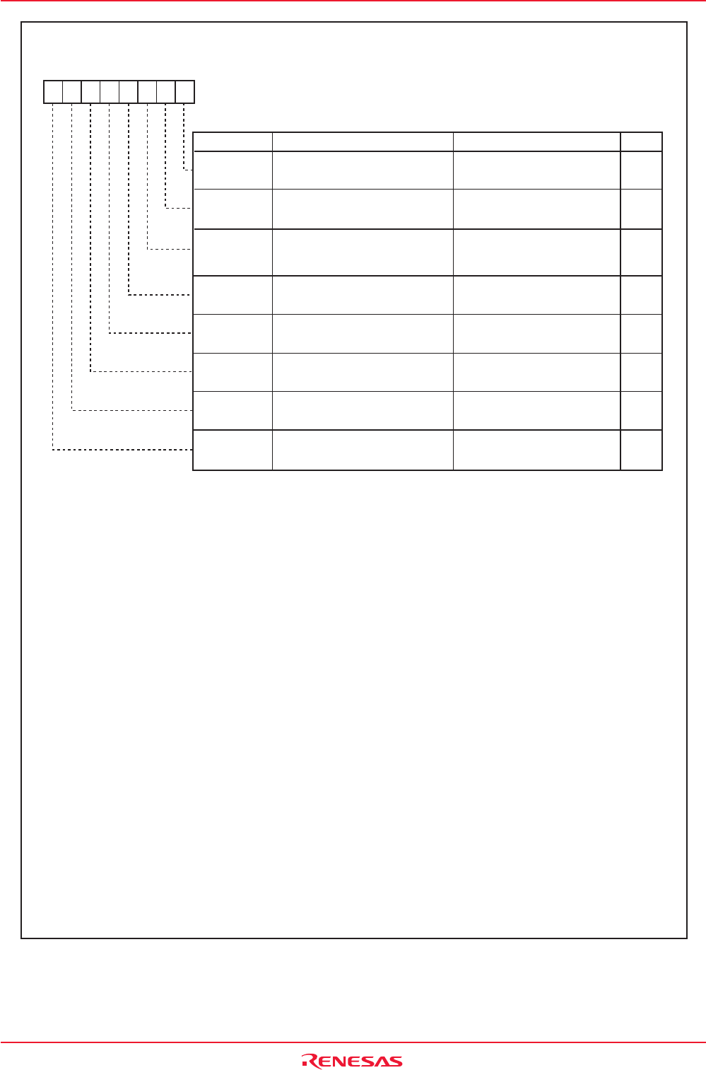
Figure 9.11 IFSR0 Register
NOTES:
1.When the IFSR16 bit in the IFSR1 register = 0, CAN1 successful transmission and SI/O3 share the
vector and interrupt control register. When using the CAN1 successful transmission interrupt, set the
IFSR00 bit to "0" (CAN1 successful transmission). When using SI/O3 interrupt, set the IFSR00 bit to
"1" (SI/O3).
2.When the PCLK6 bit in the PCLKR register = 0, A/D conversion and key input share the vector and
interrupt control register. When using the A/D conversion interrupt, set the IFSR01 bit to "0" (A/D
conversion). When using the key input interrupt, set the IFSR01 bit to "1" (key input).
3.If this bit is set to "0", the software interrupt number 1 is selected CAN0/1 wake-up and the interrupt
number 13 is selected CAN0/1 error. If this bit is set to "1", the interrupt number 1 is selected CAN0
wake-up/error and the interrupt number 13 is selected CAN1 wake-up/error.
4.When the IFSR17 bit in the IFSR1 register = 0, CAN1 successful reception and SI/O4 share the vector
and interrupt control register. When using the CAN1 successful reception interrupt, set the IFSR03 bit
to "0" (CAN1 successful reception). When using SI/O4 interrupt, set the IFSR03 bit to "1" (SI/O4).
5.Timer B5 and SI/O5 share the vector and interrupt control register. When using the timer B5 interrupt,
set the IFSR04 bit to "0" (Timer B5). When using SI/O5 interrupt, set the IFSR04 bit to "1" (SI/O5).
The SI/O5 interrupt is only in the 128-pin version. In the 100-pin version, set the IFSR04 bit to "0"
(Timer B5).
6.Timer B0 and SI/O6 share the vector and interrupt control register. When using the timer B0 interrupt,
set the IFSR05 bit to "0" (Timer B0). When using SI/O6 interrupt, set the IFSR05 bit to "1" (SI/O6).
The SI/O6 interrupt is only in the 128-pin version. In the 100-pin version, set the IFSR05 bit to "0"
(Timer B0).
7.Timer B3 and UART0 bus collision detection share the vector and interrupt control register.
When using the timer B3 interrupt, set the IFSR06 bit to "0" (Tmer B3).
When using UART0 bus collision detection, set the IFSR06 bit to "1" (UART0 bus collision detection).
8.Timer B4 and UART1 bus collision detection share the vector and interrupt control register.
When using the timer B4 interrupt, set the IFSR07 bit to "0" (Timer B4).
When using UART1 bus collision detection, set the IFSR07 bit to "1" (UART1 bus collision detection).
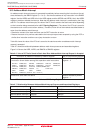
0 : CAN0/1 wake-up or error
1 : CAN0 wake-up/error or
CAN1 wake-up/error
0 : Timer B3
1 :
UART0 bus collision detection
0 : Timer B4
1 :
UART1 bus collision detection
IFSR00
IFSR01
Interrupt Request Cause
Select Bit
(1)
Interrupt Request Cause
Select Bit
(2)
IFSR02
Interrupt Request Cause
Select Bit
(3)
IFSR04
0 : Timer B0
1 : SI/O6
IFSR05
Interrupt Request Cause
Select Bit
(6)
0 : CAN1 successful reception
1 : SI/O4
Interrupt Request Cause
Select Bit
(4)
IFSR03
IFSR06
IFSR07
Interrupt Request Cause Select Register 0
Bit Symbol
b7 b6 b5 b4 b3 b2 b1 b0
Symbol Address After Reset
IFSR0 01DEh 00h
Interrupt Request Cause
Select Bit
(7)
Interrupt Request Cause
Select Bit
(8)
Function
0 : CAN1 successful transission
1 : SI/O3
0 : A/D conversion
1 : Key input
0 : Timer B5
1 : SI/O5
Interrupt Request Cause
Select Bit
(5)
RW
RW
RW
RW
RW
RW
RW
RW
RW
Bit Name