


Rev.1.10 Jul 01, 2005 page 121 of 318
REJ09B0124-0110
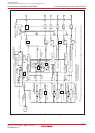
M16C/6N Group (M16C/6NK, M16C/6NM) 13. Three-Phase Motor Control Timer Function
Under development
This document is under development and its contents are subject to change.
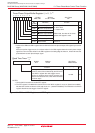
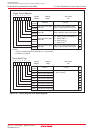
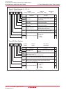
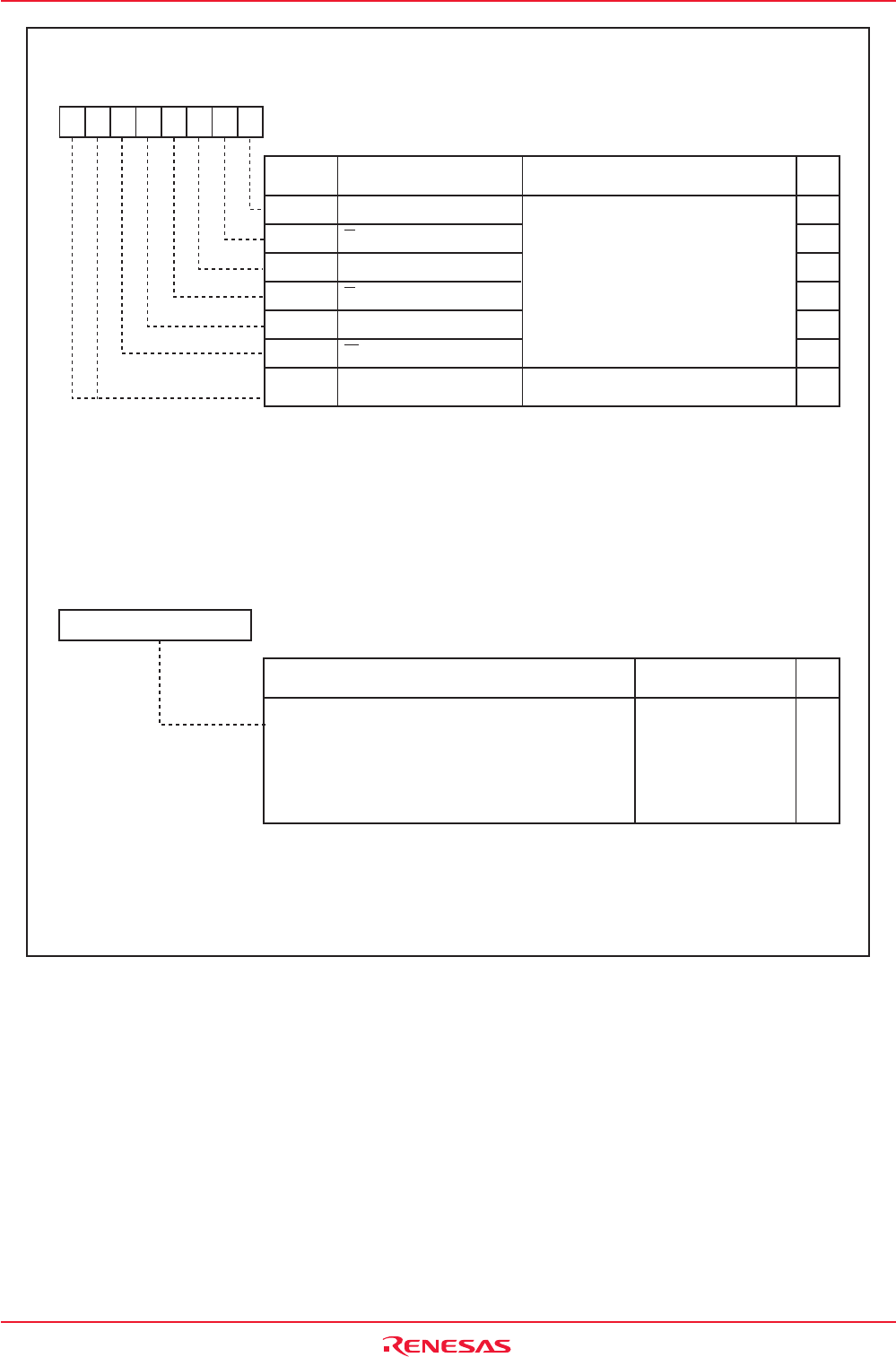
Figure 13.4 IDB0 and IDB1 Registers and DTT Register
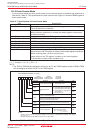
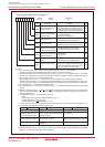
Three-Phase Output Buffer Register i (i = 0, 1)
(1)
Symbol Address After Reset
IDB0, IDB1 01CAh, 01CBh 00h
b7 b6 b5 b4 b3 b2 b1 b0
RW
RW
RW
RW
RW
RW
RW
RO
Bit Name
Bit
Symbol
DUi
DUBi
DVi
U-Phase Output Buffer i
DVBi
DWi
DWBi
-
(b7-b6)
Function
Write output level
0: Active level
1: Inactive level
When read, the value of the three-
phase shift register is read.
U-Phase Output Buffer i
V-Phase Output Buffer i
V-Phase Output Buffer i
W-Phase Output Buffer i
W-Phase Output Buffer i
NOTE:
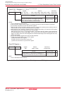
1. Values of the IDB0 and IDB1 registers are transferred to the three-phase output shift register by a transfer
trigger.
After the transfer trigger occurs, the values written in the IDB0 register determine each phase output
signal first. Then the value written in the IDB1 register on the falling edge of timers A1, A2 and A4 one-shot
pulse determines each phase output signal.
Reserved Bit Set to "0"
00
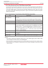
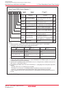
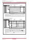
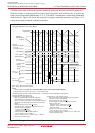
Dead Time Timer
(1) (2)
Symbol Address After Reset
DTT 01CCh Indeterminate
RW
WO
Function
b0
Setting Range
1 to 255
b7
If setting value is
n
, the timer stops when counting
n
times a count source selected by the INV12 bit
in the INVC1 register after start trigger occurs.
Positive or negative phase, which changes from
inactive level to active level, shifts when the dead
time timer stops.
NOTES:
1. Use the MOV instruction to set the DTT register.
2. The DTT register is enabled when the INV15 bit in the INVC1 register is set to "0" (dead time enabled).
No dead time can be set when the INV15 bit is set to "1" (dead time disabled). The INV06 bit in the INVC0
register determines start trigger of the DTT register.