


Rev.1.10 Jul 01, 2005 page 300 of 318
REJ09B0124-0110
M16C/6N Group (M16C/6NK, M16C/6NM) 22. Usage Precaution
Under development
This document is under development and its contents are subject to change.
22.12 A/D Converter
Set the ADCON0 (except bit 6), ADCON1 and ADCON2 registers when A/D conversion is stopped (before
a trigger occurs).
When the VCUT bit in the ADCON1 register is changed from “0” (VREF not connected) to “1” (VREF
connected), start A/D conversion after passing 1 µs or longer.
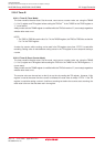
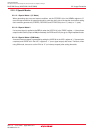
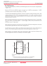
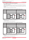
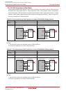
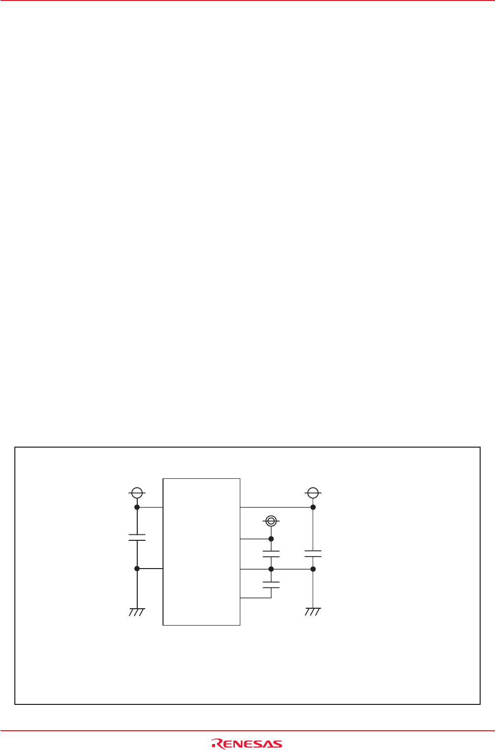
To prevent noise-induced device malfunction or latch-up, as well as to reduce conversion errors, insert
capacitors between the AVCC, VREF, and analog input pins (ANi (i = 0 to 7), AN0_i, and AN2_i) each and
the AVSS pin. Similarly, insert a capacitor between the VCC pin and the VSS pin. Figure 22.4 shows an
example connection of each pin.
Make sure the port direction bits for those pins that are used as analog inputs are set to “0” (input mode).
Also, if the TGR bit in the ADCON0 register = 1 (external trigger), make sure the port direction bit for the
__________
ADTRG pin is set to “0” (input mode).
When using key input interrupt, do not use any of the four AN4 to AN7 pins as analog inputs. (A key input
interrupt request is generated when the A/D input voltage goes low.)
The φAD frequency must be 10 MHz or less. Without sample-and-hold function, limit the φAD frequency to
250 kHz or more. With the sample and hold function, limit the φAD frequency to 1 MHz or more.
When changing an A/D operation mode, select analog input pin again in the CH2 to CH0 bits in the
ADCON0 register and the SCAN1 to SCAN0 bits in the ADCON1 register.
Figure 22.4 Use of Capacitors to Reduce Noise
VCC
VSS
C4
C1
C2
C3
Microcomputer
ANi: ANi, AN0_i, and AN2_i (i =0 to 7)
NOTES:
1. C1 ≥ 0.47 µF, C2 ≥ 0.47 µF, C3 ≥ 100 pF, C4 ≥ 0.1 µF (reference).
2. Use thick and shortest possible wiring to connect capacitors.
AVCC
AVSS
VREF
ANi