


Rev.1.10 Jul 01, 2005 page 54 of 318
REJ09B0124-0110
M16C/6N Group (M16C/6NK, M16C/6NM) 7. Clock Generating Circuit
Under development
This document is under development and its contents are subject to change.
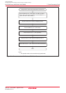
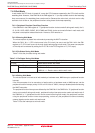
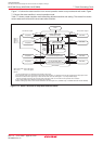
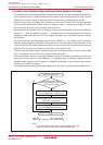
Figure 7.12 State Transition to Stop Mode and Wait Mode
Stop Mode
Reset
Normal Mode
PLL Operation Mode
High-Speed Mode,
Medium-Speed Mode
Medium-Speed Mode
(divided-by-8 mode)
Low-Speed Mode,
Low Power Dissipation Mode
Stop Mode
Wait Mode
Wait Mode
Stop Mode
WAIT
instruction
WAIT
instruction
WAIT
instruction
WAIT
instruction
CPU operation stoppedAll oscillators stopped
CM05, CM06, CM07: Bits in CM0 register
CM10, CM11: Bits in CM1 register
NOTES:
1.
Do not go directly from PLL operation mode to wait or stop mode.
2.PLL operation mode can be entered from high-speed mode. Similarly, PLL operation mode can be changed back to high-speed mode.
3.Write to the CM0 and CM1 registers per 16 bits with the CM21 bit in the CM2 register = 0 (on-chip oscillator stops).
Since the operation starts from the main clock after exiting stop mode, the time until the CPU operates can be reduced.
4.The on-chip oscillator clock divided by 8 provides the CPU clock.
5.Before entering stop mode, be sure to set the CM20 bit in the CM2 register to "0" (oscillation stop, re-oscillation detection function disabled).
Interrupt
CM10 = 1
(5)
CM07 = 0
CM06 = 1
CM05 = 0
CM11 = 0
CM10 = 1
(3)
CM10 = 1
(5)
Interrupt
CM10 = 1
(5)
Interrupt
Interrupt
Interrupt
(NOTES 1, 2)
Wait Mode
Interrupt
When
low
power
dissipation
mode
When
low-
speed
mode
On-chip Oscillator Mode,
On-chip Oscillator Dissipation Mode
Stop Mode
CM10 = 1
(5)
Interrupt
(4)
Wait Mode
Interrupt
Figure 7.12 shows the state transition from normal operation mode to stop mode and wait mode. Figure
7.13 shows the state transition in normal operation mode.
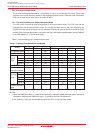
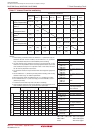
Table 7.7 shows a state transition matrix describing allowed transition and setting. The vertical line shows
current state and horizontal line show state after transition.