


Rev.1.10 Jul 01, 2005 page 126 of 318
REJ09B0124-0110
M16C/6N Group (M16C/6NK, M16C/6NM) 13. Three-Phase Motor Control Timer Function
Under development
This document is under development and its contents are subject to change.
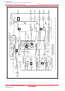
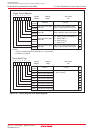
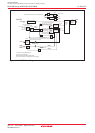
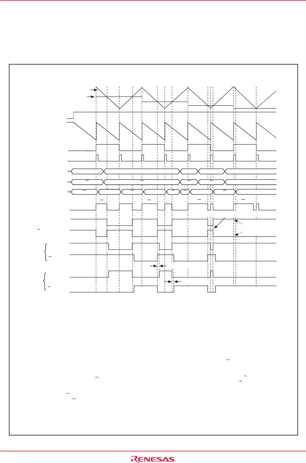
Figure 13.9 Triangular Wave Modulation Operation
The three-phase motor control timer function is enabled by setting the INV02 bit in the INVC0 register to “1”.
When this function is selected, timer B2 is used to control the carrier wave, and timers A4, A1 and A2 are
__ ___ ___
used to control three-phase PWM outputs (U, U, V, V, W and W). The dead time is controlled by a dedicated
dead-time timer. Figure 13.9 shows the example of triangular modulation waveform and Figure 13.10
shows the example of sawtooth modulation waveform.
TA4 register
(2)
TA4-1 register
(2)
Reload register
(2)
m
m
m
nn
p
p
p
m
m
q
q
q
Timer A1
reload control signal
(1)
m n n
n
n
n p
p
q
qp
q
r
r
Triangular Wave
Signal Wave
Triangular waveform as a Carrier Wave
Timer B2
TB2S bit in
TABSR register
Timer A4
start trigger signal
(1)
Timer A4
one-shot pulse
(1)
Rewrite the IDB0 and IDB1 registers
Transfer a counter
value to the three-phase
shift register
U-phase output
signal
(1)
U-phase output
signal
(1)
U-phase
INV14 = 0
("L" active)
U-phase
Dead time
Dead time
INV14 = 1
("H" active)
U-phase
U-phase
NOTES:
1.Internal signals. See Figure 13.1 Three-Phase Motor Control Timer Functions Block Diagram.
2.Applies only when the INV11 bit is set to "1" (three-phase mode).
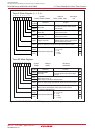
Examples of PWM output change are
(a) When INV11=1 (three-phase mode 1)
- INV01=0 and ICTB2=2h (The timer B2 interrupt is
generated with every second timer B2 underflow) or
INV01= 1, INV00=1 and ICTB2=1h (The timer B2 interrupt is
generated on the falling edge of the timer A reload control
signal)
- Default value of the timer: TA41=m, TA4=m
The TA4 and TA41 registers are changed whenever the
timer B2 interrupt is generated.
First time: TA41=n, TA4=n.
Second time: TA41=p, TA4=p.
- Default value of the IDB0 and IDB1 registers
DU0=1, DUB0=0, DU1=0, DUB1=1
They are changed to DU0=1, DUB0=0, DU1=1, DUB1=0
by the third timer B2 interrupt.
(b) When INV11=0 (three-phase mode 0)
- INV01=0, ICTB2=1h (The timer B2 interrupt is generated
whenever the timer B2 underflows)
- Default value of the timer: TA4=m
The TA4 register is changed whenever the timer B2
interrupt is generated.
First time: TA4=m. Second time: TA4=n.
Third time: TA4=n. Fourth time: TA=p.
Fifth time: TA4=p.
- Default value of the IDB0 and IDB1 registers:
DU0=1, DUB0=0, DU1=0, DUB1=1
They are changed to DU0=1, DUB0=0, DU1=1, DUB1=0 by
the sixth timer B2 interrupt.
The above applies to INVC0 = 00XX11XXb and INVC1 = 010XXXX0b (X varies depending on each system.)
INV00, INV01: Bits in the INVC0 register
INV11, INV14: Bits in the INVC1 register