


Rev.1.10 Jul 01, 2005 page 193 of 318
REJ09B0124-0110
M16C/6N Group (M16C/6NK, M16C/6NM) 15. A/D Converter
Under development
This document is under development and its contents are subject to change.
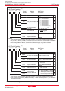
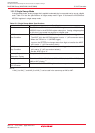
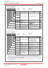
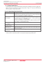
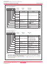
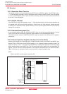
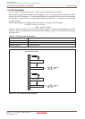
Item Specification
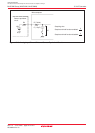
Function The input voltages on all pins selected by the ADGSEL1 to ADGSEL0 bits
in the ADCON2 register are A/D converted repeatedly, with priority given
to pins selected by the SCAN1 to SCAN0 bits in the ADCON1 register and
ADGSEL1 to ADGSEL0 bits.
Example : If AN0 selected, input voltages are A/D converted in order of
AN0 AN1 AN0 AN2 AN0 AN3, and so on.
A/D Conversion • When the TRG bit in the ADCON0 register is “0” (software trigger)
Start Condition The ADST bit in the ADCON0 register is set to “1” (A/D conversion starts)
_____________
• When the TRG bit is “1” (ADTRG trigger)
_____________
Input on the ADTRG pin changes state from high to low after the ADST
bit is set to “1” (A/D conversion starts)
A/D Conversion Set the ADST bit to “0” (A/D conversion halted)
Stop Condition
Interrupt Request None generated
Generation Timing
Analog Input Pins to be Given
Select from AN0 (1 pin), AN0 to AN1 (2 pins), AN0 to AN2 (3 pins),
Priority when A/D Converted
AN0 to AN3 (4 pins)
(1)
Reading of Result of Read one of the AD0 to AD7 registers that corresponds to the selected pin
A/D Converter
NOTE:
1. AN0_0 to AN0_7, and AN2_0 to AN2_7 can be used in the same way as AN0 to AN7.
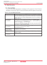
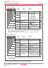
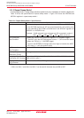
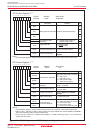
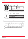
15.1.5 Repeat Sweep Mode 1
In repeat sweep mode 1, analog voltage selectively applied to all pins is repeatedly converted to a digital code.
Table 15.6 lists the specifications of repeat sweep mode 1. Figure 15.8 shows the ADCON0 and
ADCON1 registers in repeat sweep mode 1.
Table 15.6 Repeat Sweep Mode 1 Specifications