


Rev.1.10 Jul 01, 2005 page 129 of 318
REJ09B0124-0110
M16C/6N Group (M16C/6NK, M16C/6NM) 14. Serial I/O
Under development
This document is under development and its contents are subject to change.
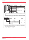
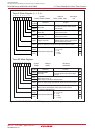
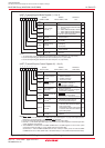
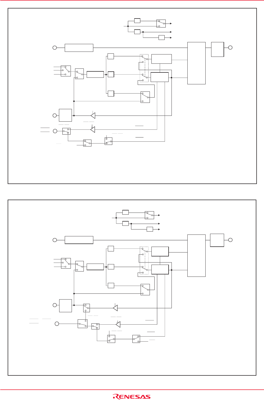
Figure 14.1 UART0 Block Diagram
RXD0
1 / (n0+1)
1/16
1/16
1/2
U0BRG
register
Clock synchronous type
(when internal clock is selected)
Clock synchronous
type
Clock synchronous type
(when internal clock is selected)
Clock synchronous
type
(when external clock
is selected)
CLK0
Clock source selection
CTS0 /
RTS0
f1SIO or f2SIO
f8SIO
f32SIO
Internal
External
RTS0
CTS0
TXD0
Transmit/
receive
unit
(UART0)
CLK1 to CLK0
00h
01h
10h
CKDIR
CKPOL
UART reception
UART transmission
Clock synchronous type
CKDIR
1
0
RXD polarity
reversing circuit
0
1
RCSP
1
VSS
0
1
PCLK1
f1SIO or f2SIO
1/2
Main clock, PLL clock, or on-chip oscillator clock
1/2
1/8
f8SIO
f32SIO
f1SIO
f2SIO
0
1
SMD2 to SMD0
010, 100, 101, 110
001
010, 100, 101, 110
001
0
1
CRS
0
CRD
1/4
Receive
clock
Transmit
clock
Reception
control circuit
Transmission
control circuit
TXD
polarity
reversing
circuit
CTS/RTS disabled
CTS/RTS disabled
CTS/RTS selected
CTS
0
from UART1
CLK
polarity
reversing
circuit
n0: Values set to the U0BRG register
PCLK1: Bit in PCLKR register
SMD2 to SMD0, CKDIR: Bits in U0MR register
CLK1 to CLK0, CKPOL, CRD, CRS: Bits in U0C0 register
RCSP: Bit in UCON register
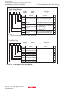
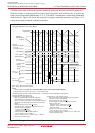
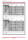
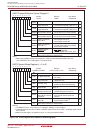
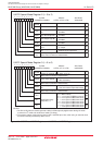
Figure 14.2 UART1 Block Diagram
RXD1
Reception
control circuit
Transmission
control circuit
1 / (n1+1)
1/16
1/16
1/2
U1BRG
register
Clock synchronous type
(when internal clock is selected)
Clock synchronous
type
Clock synchronous type
(when internal clock is selected)
Clock synchronous type
(when external clock is selected))
CLK1
Clock source selection
f1SIO or f2SIO
f8SIO
f32SIO
Internal
External
TXD1
(UART1)
CLK1 to CLK0
00
01
10
CKDIR
UART reception
UART transmission
Clock synchronous
type
CKDIR
RXD polarity reversing
circuit
0
1
SMD2 to SMD0
010, 100, 101, 110
001
010, 100, 101, 110
001
0
1
RTS1
CTS1
Clock output
pin select
CTS1 / RTS1/
CTS0 / CLKS1
VSS
CRD
1
0
0
CRS
0
0
1
CLKMD0
1
CLK
polarity
reversing
circuit
CKPOL
1
CLKMD1
1
0
RCSP
n1: Values set to the U1BRG register
PCLK1: Bit in PCLKR register
SMD2 to SMD0, CKDIR: Bits in U1MR register
CLK1 to CLK0, CKPOL, CRD, CRS: Bits in U1C0 register
CLKMD0, CLKMD1, RCSP: Bits in UCON register
PCLK1
f1SIO or f2SIO
1/2
Main clock, PLL clock, or on-chip oscillator clock
1/2
1/8
f8SIO
f32SIO
f1SIO
f2SIO
0
1
1/4
Receive
clock
Transmit
clock
Transmit/
receive
unit
TXD
polarity
reversing
circuit
CTS0 from UART0
CTS/RTS disabled
CTS/RTS disabled
CTS/RTS selected