


Rev.1.10 Jul 01, 2005 page 155 of 318
REJ09B0124-0110
M16C/6N Group (M16C/6NK, M16C/6NM) 14. Serial I/O
Under development
This document is under development and its contents are subject to change.
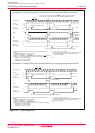
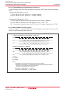
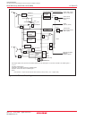
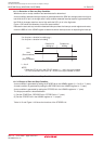
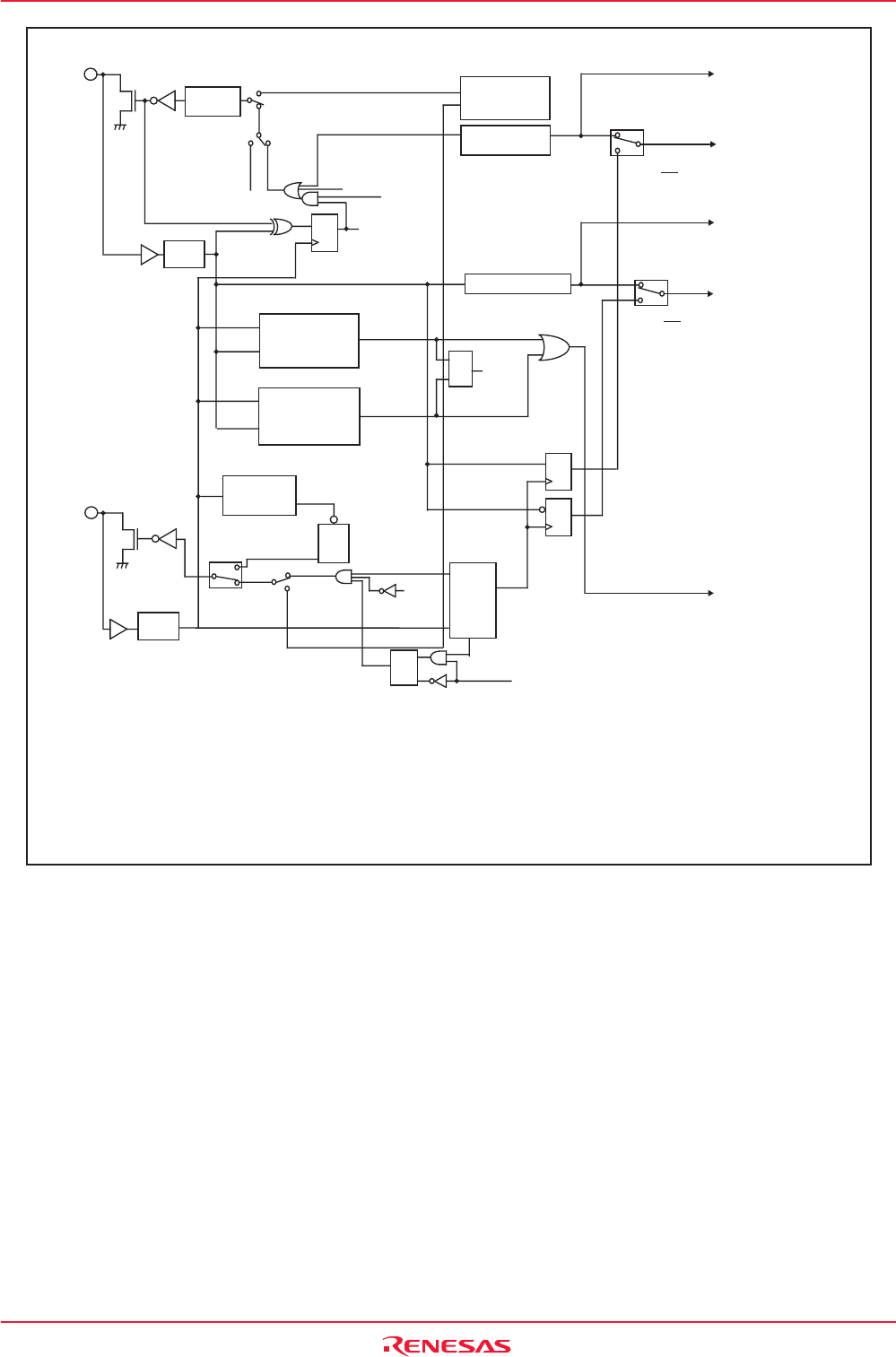
Figure 14.23 I
2
C Mode Block Diagram
CLK
control
Falling edge
detection
External
clock
Internal clock
Start/stop condition
detection
interrupt request
Start condition
detection
Stop condition
detection
Reception register
Bus
busy
Transmission
register
Arbitration
Noise
Filter
SDAi
SCLi
UARTi
D
T
Q
D
T
Q
D
T
Q
NACK
ACK
UARTi
UARTi
UARTi
R
UARTi transmit,
NACK interrupt
request
UARTi receive,
ACK interrupt request,
DMA1 request
IICM=1 and
IICM2=0
S
R
Q
ALS
R
S
SWC
IICM=1 and
IICM2=0
IICM2=1
IICM2=1
SWC2
SDHI
DMA0, DMA1 request
(UART1: DMA0 only)
Noise
Filter
IICM=0
IICM=1
DMA0
(UART0, UART2)
STSPSEL=0
STSPSEL=1
STSPSEL=1
STSPSEL=0
SDA(STSP)
SCL(STSP)
ACKC=1
ACKC=0
Q
Port register
(1)
I/O port
9th bit falling edge
9th bit
ACKD bit
Delay
circuit
Start and stop condition generation block
This diagram applies to the case where the SMD2 to SMD0 bits in the UiMR register = 010b and the IICM bit in the UiSMR register = 1.
i = 0 to 2
IICM: Bit in UiSMR register
IICM2, SWC, ALS, SWC2, SDHI: Bits in UiSMR2 register
STSPSEL, ACKD, ACKC: Bits in UiSMR4 register
NOTE:
1. If the IICM bit =1, the pins can be read even when the PD6_2, PD6_6 or PD7_1 bit = 1 (output mode).