


Rev.1.10 Jul 01, 2005 page 117 of 318
REJ09B0124-0110
M16C/6N Group (M16C/6NK, M16C/6NM) 13. Three-Phase Motor Control Timer Function
Under development
This document is under development and its contents are subject to change.
13. Three-Phase Motor Control Timer Function
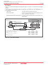
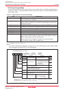
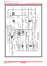
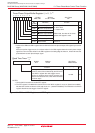
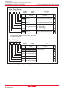
Timers A1, A2, A4 and B2 can be used to output three-phase motor drive waveforms. Table 13.1 lists the
specifications of the three-phase motor control timer function. Figure 13.1 shows the block diagram for three-phase
motor control timer function. Also, the related registers are shown on Figures 13.2 to 13.8.
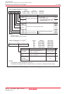
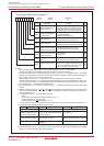
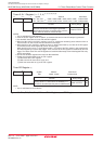
Table 13.1 Three-Phase Motor Control Timer Function Specifications
Item Specification
Three-Phase Waveform Output Pin
___ ___ ___
Six pins (U, U, V, V, W, W)
Forced Cutoff Input
(1)
_______
Input “L” to NMI pin
Used Timers Timer A4, A1, A2 (used in the one-shot timer mode)
___
• Timer A4: U- and U-phase waveform control
___
• Timer A1: V- and V-phase waveform control
___
• Timer A2: W- and W-phase waveform control
Timer B2 (used in the timer mode)
• Carrier wave cycle control
Dead time timer (3 eight-bit timer and shared reload register)
• Dead time control
Output Waveform Triangular wave modulation, Sawtooth wave modification
• Enable to output “H” or “L” for one cycle
•
Enable to set positive-phase level and negative-phase level respectively
Carrier Wave Cycle Triangular wave modulation: count source ✕ (m+1) ✕ 2
Sawtooth wave modulation: count source ✕ (m+1)
m: Setting value of the TB2 register, 0 to 65535
Count source: f1, f2, f8, f32, fC32
Three-Phase PWM Output Width Triangular wave modulation: count source ✕ n ✕ 2
Sawtooth wave modulation: count source ✕ n
n: Setting value of the TA4, TA1 and TA2 registers (of the TA4,
TA41, TA1, TA11, TA2 and TA21 registers when setting the
INV11 bit to “1”), 1 to 65535
Count source: f1, f2, f8, f32, fC32
Dead Time Count source ✕ p, or no dead time
p: Setting value of the DTT register, 1 to 255
Count source: f1, f2, f1 divided by 2, f2 divided by 2
Active Level Enable to select “H” or “L”
Positive and Negative-Phase Concurrent
Positive and negative-phases concurrent active disable function
Active Disable Function Positive and negative-phases concurrent active detect function
Interrupt Frequency For Timer B2 interrupt, select a carrier wave cycle-to-cycle basis
through 15 times carrier wave cycle-to-cycle basis
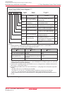
NOTE:
1.
_______
Forced cutoff with NMI input is effective when the IVPCR1 bit in the TB2SC register is set to “1” (three-phase
_______ _______
output forcible cutoff by NMI input enabled). If an “L” signal is applied to the NMI pin when the IVPCR1
bit is “1”, the related pins go to a high-impedance state regardless of which functions of those pins are
being used.
Related pins: • P7_2/CLK2/TA1OUT/V
_________ _________ ___
• P7_3/CTS2/RTS2/TA1IN/V
• P7_4/TA2OUT/W/(CLK4)
____
• P7_5/TA2IN/W/(SOUT4)
• P8_0/TA4OUT/U(SIN4)
___
• P8_1/TA4IN/U