


Rev.1.10 Jul 01, 2005 page 263 of 318
REJ09B0124-0110
M16C/6N Group (M16C/6NK, M16C/6NM) 20. Flash Memory Version
Under development
This document is under development and its contents are subject to change.
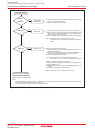
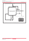
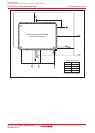
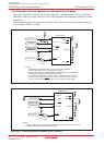
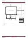
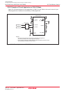
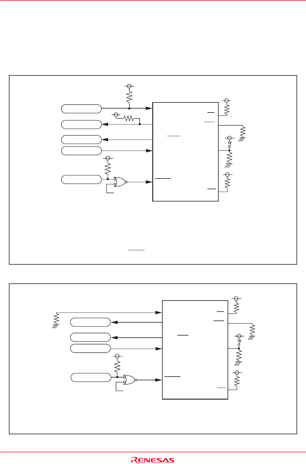
20.4.2 Example of Circuit Application in Standard Serial I/O Mode
Figures 20.15 and 20.16 show example of circuit application in standard serial I/O mode 1 and mode 2,
respectively. Refer to the user’s manual of your serial programmer to handle pins controlled by a serial
programmer.
Note that when using the standard serial I/O mode 2, make sure a main clock input oscillation frequency
is set to 5 MHz, 10 MHz or 16 MHz.
Figure 20.15 Circuit Application in Standard Serial I/O Mode 1
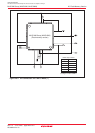
Figure 20.16 Circuit Application in Standard Serial I/O Mode 2
Microcomputer
NOTES:
1.Control pins and external circuitry will vary according to programmer.
For more information, refer to the programmer manual.
2.In this example, modes are switched between single-chip mode and standard serial
I/O mode by controlling the CNVSS input with a switch.
3.If in standard standard serial I/O mode 1 there is a possibility that the user reset
signal will go low during standard serial I/O mode, break the connection between
the user reset signal and RESET pin by using, for example, a jumper switch.
SCLK input
BUSY output
TXD output
RXD input
Reset input
P6_4/RTS1
P6_6/CLK1
P6_7/TXD1
RESET
P6_6/RXD1
CNVSS
P5_0(CE)
P5_5(EPM)
P8_5/NMI
User reset
signal
Microcomputer
P6_4/RTS1
P6_5/CLK1
P6_7/TXD1
P6_6/RXD1
CNVSS
P5_0(CE)
P5_5(EPM)
P8_5/NMI
Monitor output
TXD output
RXD input
NOTES:
1.In this example, modes are switched between single-chip mode and standard serial I/O
mode by controlling the CNVSS input with a switch.
Reset input
RESET
User reset
signal