


Rev.1.10 Jul 01, 2005 page 256 of 318
REJ09B0124-0110
M16C/6N Group (M16C/6NK, M16C/6NM) 20. Flash Memory Version
Under development
This document is under development and its contents are subject to change.
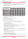
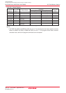
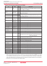
Table 20.5 Status Register
SR7 (D7)
SR6 (D6)
SR5 (D5)
SR4 (D4)
SR3 (D3)
SR2 (D2)
SR1 (D1)
SR0 (D0)
Sequencer status
Reserved
Erase status
Program status
Reserved
Reserved
Reserved
Reserved
Busy
-
Terminated normally
Terminated normally
-
-
-
-
Ready
-
Terminated in error
Terminated in error
-
-
-
-
“0”
Status Name
Contents
Bits in Status
Register
“1”
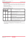
FMR00
-
FMR07
FMR06
-
-
-
-
Bits in FMR0
Register
Value after
Reset
1
-
0
0
-
-
-
-
D7 to D0: These data bus are read when the read status register command is executed.
NOTE:
1. The FMR07 bit (SR5) and FMR06 bit (SR4) are set to “0” by executing the clear status register command.
When the FMR07 bit (SR5) or FMR06 bit (SR4) is set to “1”, the program, block erase, erase all
unlocked block, and lock bit program commands are not accepted.