


Rev.1.10 Jul 01, 2005 page 123 of 318
REJ09B0124-0110
M16C/6N Group (M16C/6NK, M16C/6NM) 13. Three-Phase Motor Control Timer Function
Under development
This document is under development and its contents are subject to change.
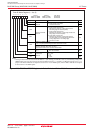
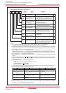
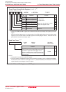
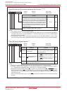
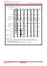
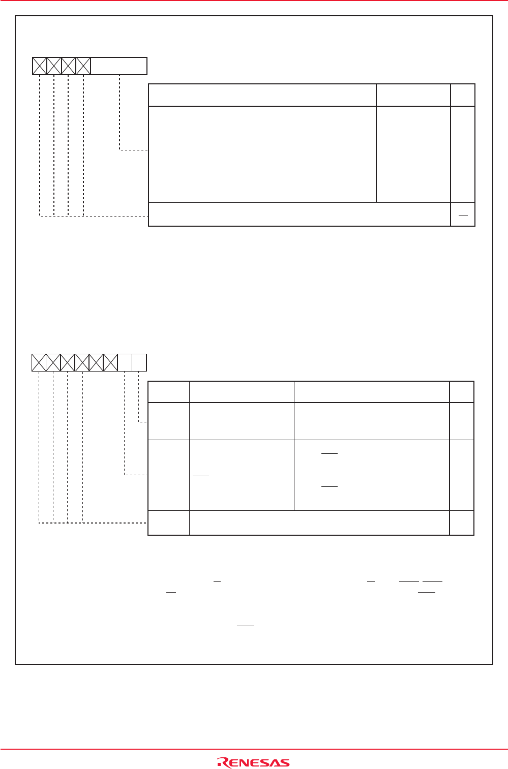
Figure 13.6 ICTB2 Register and TB2SC Register
Timer B2 Interrupt Occurrence Frequency Set Counter
(1) (2) (3)
Symbol Address After Reset
ICTB2 01CDh Indeterminate
b7 b0
RW
WO
Function
Setting Range
1 to 15
Nothing is assigned. When write, set to "0".
When the INV01 bit in the INVC0 register is set to "0"
(the ICTB2 counter
increments whenever the timer B2
underflows) and the
setting value is
n
, the timer B2 interrupt
is generated
every
n
th time timer B2 underflow occurs.
When the INV01 bit is set to "1" (the INV00 bit selects
count timing of the ICTB2 counter) and setting value is
n
, the timer B2 interrupt is generated every
n
th time
timer B2 underflow meeting the condition selected in
the INV00 bit occurs.
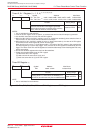
NOTES:
1. Use the MOV instruction to set the ICTB2 register.
2. If the INV01 bit is set to "1", set the ICTB2 register when the TB2S bit is set to "0" (timer B2 counter stopped),
If the INV01 bit is set to "0" and the TB2S bit to "1" (timer B2 counter start), do not set the ICTB2 register
when the timer B2 underflows.
3.If the INV00 bit is set to "1", the first interrupt is generated when the timer B2 underflows
n-1
times,
n
being
the value set in the ICTB2 counter. Subsequent interrupts are generated every
n
times the timer B2 underflows.
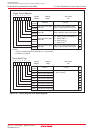
Timer B2 Reload Timing
Switching Bit
Nothing is assigned. When write, set to "0".
When read, their contents are "0".
PWCOM
IVPCR1
-
(b7-b2)
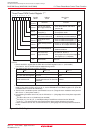
Timer B2 Special Mode Register
(1)
Symbol Address After Reset
TB2SC 039Eh XXXXXX00b
b7 b6 b5 b4 b3 b2 b1 b0
RW
RW
RW
-
NOTES:
1. Write to this register after setting the PRC1 bit in the PRCR register to "1" (write enabled).
2. If the INV11 bit in the INVC1 register is "0" (three-phase mode 0) or the INV06 bit in the INVC0 register
is "1" (sawtooth wave modulation mode), set this bit to "0" (timer B2 underflow).
3.Related pins are U(P8_0/TA4OUT/(SIN4)), U(P8_1/TA4IN), V(P7_2/CLK2/TA1OUT), V(P7_3/CTS2/RTS2/TA1IN),
W(P7_4/TA2OUT/(CLK4)), W(P7_5/TA2IN/(SOUT4)). If a low-level signal is applied to the NMI pin when
the IVPCR1 bit = 1, the target pins go to a high-impedance state regardless of which functions of those
pins are being used.
After forced interrupt (cutoff), input "H" to the NMI pin and set the IVPCR1 bit to "0": this forced cutoff will
be reset.
Bit Name
Bit
Symbol
Function
0 : Timer B2 underflow
1 : Timer A output at odd-numbered
occurrences
(2)
Three-Phase Output Port
NMI Control Bit 1
(3)
0 : Three-phase output forcible cutoff
by NMI input (high-impedance)
disabled
1 : Three-phase output forcible cutoff
by NMI input (high-impedance)
enabled