


Rev.1.10 Jul 01, 2005 page 107 of 318
REJ09B0124-0110
M16C/6N Group (M16C/6NK, M16C/6NM) 12. Timers
Under development
This document is under development and its contents are subject to change.
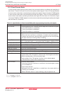
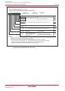
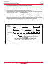
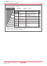
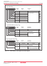
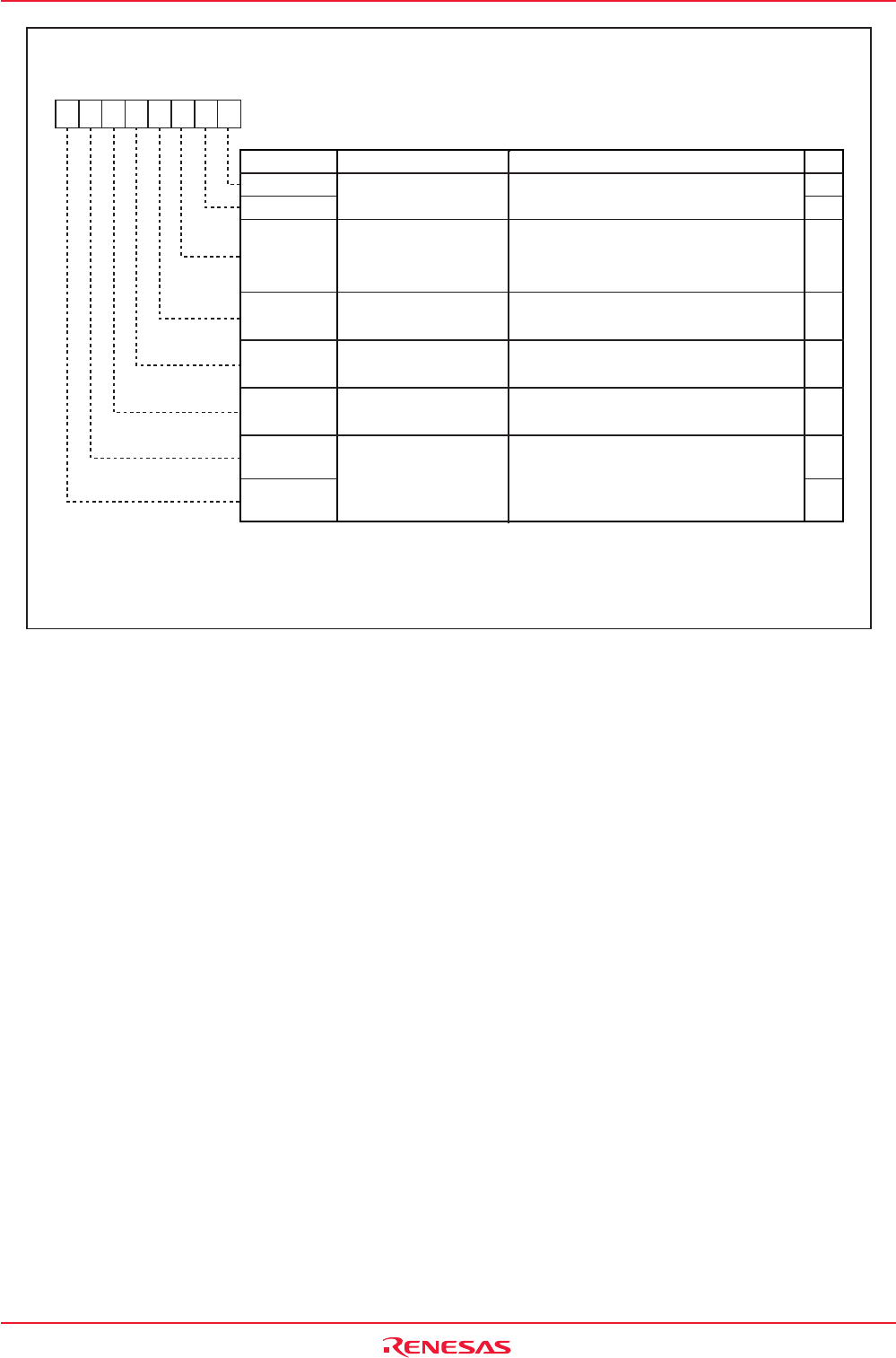
Figure 12.12 TA0MR to TA4MR Registers in Pulse Width Modulation Mode
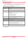
Bit Name
Timer Ai Mode Register (i = 0 to 4)
FunctionBit Symbol
b7 b6 b5 b4 b3 b2 b1 b0
Operation Mode
Select Bit
Pulse Output Function
Select Bit
(3)
1 1 : Pulse width modulation mode
b1 b0
TMOD1
TMOD0
MR0
RW
111
RW
RW
RW
After Reset
00h
Address
0396h to 039Ah
Symbol
TA0MR to TA4MR
MR2
MR1
MR3
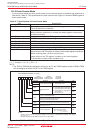
b7 b6
TCK1
TCK0
Count Source Select Bit
16/8-Bit Pulse Width
Modulation Mode Select Bit
Trigger Select Bit
External Trigger Select
Bit
(1)
RW
RW
RW
RW
RW
1 : Selected by TAiTGH to TAiTGL bits
0 : Falling edge of input signal to TAiIN pin
(2)
1 : Rising edge of input signal to TAiIN pin
(2)
0 : Pulse is not output
(TAiOUT pin is a normal port pin)
1 : Pulse is output
(TAiOUT pin is a pulse output pin)
0 :
Functions as a 16-bit pulse width modulator
1 :
Functions as an 8-bit pulse width modulator
0 : Write "1" to TAiS bit in the TABSR register
0 0 : f1 or f2
0 1 : f8
1 0 : f32
1 1 : fC32
NOTES:
1.Effective when the TAiTGH and TAiTGL bits in the ONSF or TRGSR register are "00b" (TAiIN pin input).
2.The port direction bit for the TAiIN pin is set to "0" (input mode).
3.Set to "1" (pulse is output), PWM pulse is output.