CLOCK & POWER MANAGEMENT S3C2440A RISC MICROPROCESSOR
7-10
POWER MANAGEMENT
The Power Management block controls the system clocks by software for the reduction of power consumption in
the S3C2440A. These schemes are related to PLL, clock control logics (FCLK, HCLK, and PCLK) and wakeup
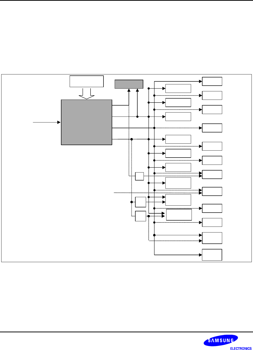
signals. Figure 7-7 shows the clock distribution of the S3C2440A.
The S3C2440A has four power modes. The following section describes each power management mode. The
transition between the modes is not allowed freely. Please see Figure 7-8 for available transitions among the
modes.
INTCNTL
Power
Management
FCLK
Input Clock
FCLK defination
If SLOW mode
FCLK = input clock/divider ratio
If Normal mode (P, M & S value)
FCLK = MPLL clock (Mpll)
ARM920T
HCLK
PCLK
UPLL(96/48 MHz)
BUSCNTL
MEMCNTL
ARB/DMA
ExtMaster
LCDCNTL
Nand Flash
Controller
Camera
WDT
SPI
PWM
I2C
SDI
ADC
UART
I2S
GPIO
RTC
USB
Device
Clock Control
Register
USB
Host I/F
1/d
1/2
1/1
AC97
1/n
MPLLin
Figure 7-7. The Clock Distribution Block Diagram


