


S3C2440A RISC MICROPROCESSOR ELECTRICAL DATA
27-3
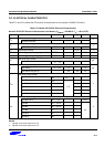
D.C. ELECTRICAL CHARACTERISTICS
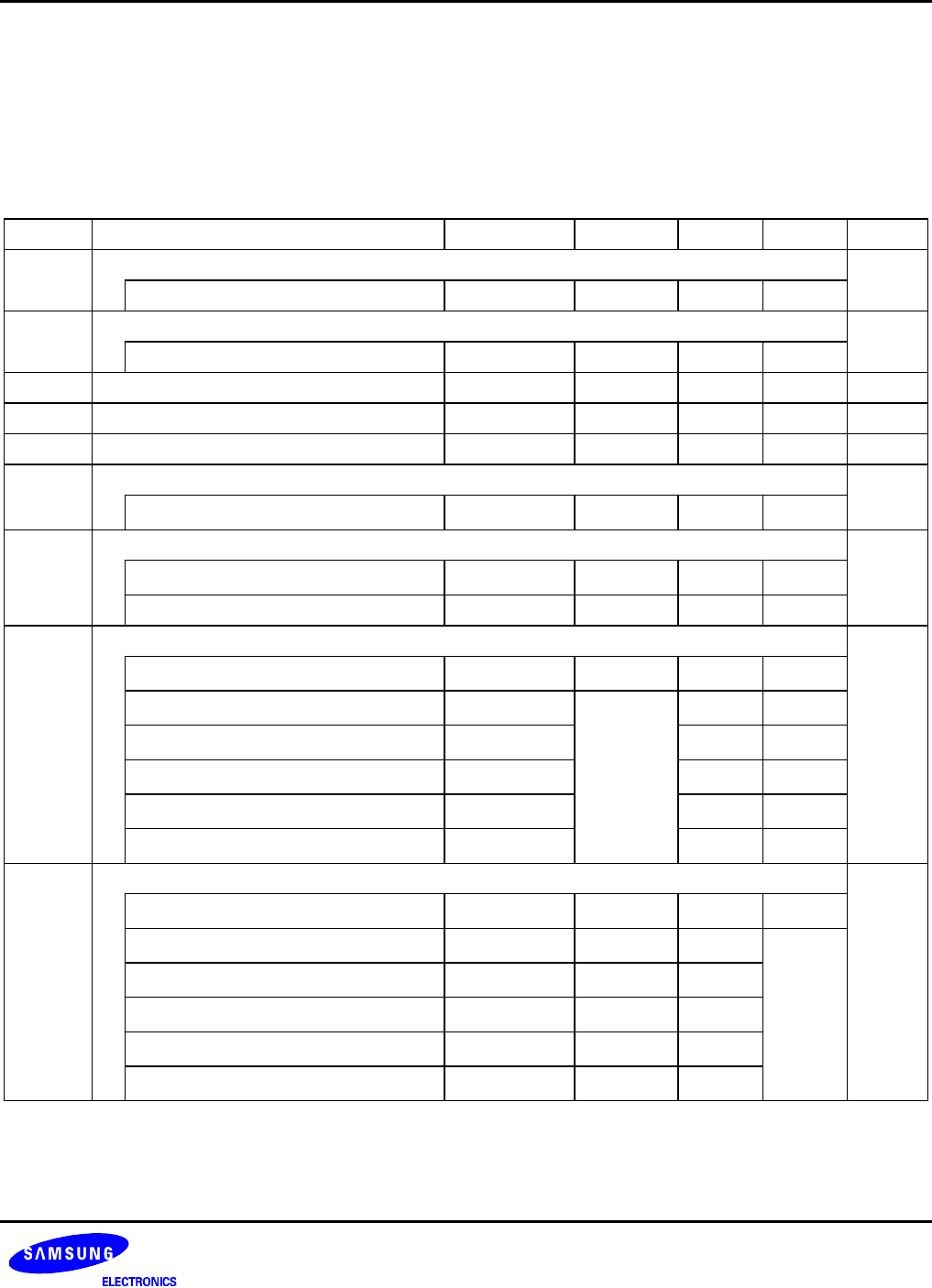
Table 27-3 and 27-4 defines the DC electrical characteristics for the standard LVCMOS I/O buffers.
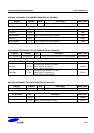
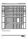
Table 27-3 Normal I/O PAD DC Electrical Characteristics
Normal I/O PAD DC Electrical Characteristics for Memory (V
DDMOP
= 2.5V±
±±
±0.2V, T
A
= -40 to 85 °
°°
°C)
Symbol Parameters Condition Min Typ. Max Unit
High level input voltage
V
IH
LVCMOS interface 1.7
V
Low level input voltage
V
IL
LVCMOS interface 0.7
V
VT Switching threshold 0.5V
DD
V
VT+ Schmitt trigger, positive-going threshold CMOS 2.0 V
VT- Schmitt trigger, negative-going threshold CMOS 0.8 V
High level input current
I
IH
Input buffer
V
IN
= V
DD
-10
10
µA
Low level input current
Input buffer
V
IN
= V
SS
-10
10
I
IL
Input buffer with pull-up -60 -33 -10
µA
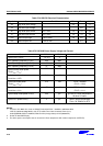
High level output voltage
Type B4 to B12
I
OH
= - 1 µA V
DD
-0.05
Type B4
I
OH
= - 4 mA
Type B6
I
OH
= - 6 mA
Type B8
I
OH
= - 8 mA
Type B10
I
OH
= -10 mA
V
OH
Type B12
I
OH
= -12 mA
2.0
V
Low level output voltage
Type B4 to B12
I
OL
= 1 µA
0.05
Type B4
I
OL
= 4 mA
Type B6
I
OL
= 6 mA
Type B8
I
OL
= 8 mA
Type B10
I
OL
= 10 mA
V
OL
Type B12
I
OL
= 12 mA
0.4
V
NOTES:
1. Type B6 means 6mA output driver cell.
2. Type B8 means 8mA output driver cell.