AC97 CONTROLLER S3C2440A RISC MICROPROCESSOR
24-6
AC-LINK INPUT FRAME (SDATA_IN)
SDATA_OUT
BIT_CLK
SYNC
AC '97 samples SYNC assertion here
AC '97 Controller samples first SDATA_IN bit of frame here
END of previous Audio Frame
Codec
Ready
Slot(1) Slot(2)
Slot(12) "0" "0" "0" 19 0
Tag Phase Data Phase
19 0
START of Data phase
Slot# 1
END of Data Frame
Slot# 12
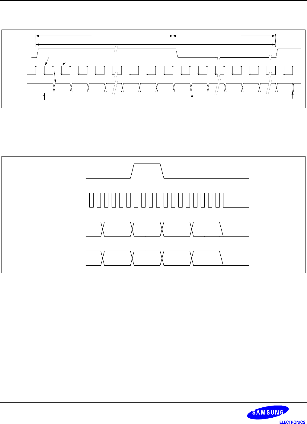
Figure 24-6 AC-link Input Frame
AC97 POWERDOWN
SDATA_OUT
SDATA_IN
BIT_CLK
SYNC
slot 12
prev.frame
Write to
0X26
slot 12
prev.frame
TAG
TAG
Data
PR4
Figure 24-7 AC97 Powerdown Timing Diagram
Powering Down the AC-link
The AC-link signals enter a low power mode when the AC97 CODEC Powerdown register (0x26) bit PR4 is set to
1 (i.e. by writing 0x1000). Then the Primary CODEC drives both the BITCLK and SDATA_IN to a logic low voltage
level. The sequence follows the timing diagram shown above in the Figure 24-7.
The AC97 Controller transmits the write to Powerdown register (0x26) over the AC-link. Set up the AC97 Controller
so that it does not transmit data to slots 3-12 when it writes to the Powerdown register bit PR4 (data 0x1000), and
it does not require the CODEC to process other data when it receives a power down request. When the CODEC
processes the request, it immediately transitions BITCLK and SDATA_IN to a logic low level. The AC97 Controller
drives the SYNC and SDATA_OUT to a logic low level after programming the AC_GLBCTRL register.


