


PRODUCT OVERVIEW S3C2440A RISC MICROPROCESSOR
1-26
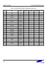
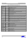
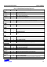
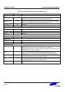
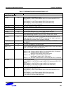
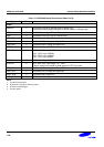
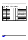
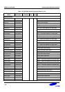
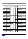
Table 1-3. S3C2440A Signal Descriptions (Sheet 6 of 6)
Signal Input/Output Description
Power
VDDalive P S3C2440A reset block and port status register VDD.
It should be always supplied whether in normal mode or in Sleep mode.
VDDiarm P S3C2440A core logic VDD for ARM core.
VDDi P S3C2440A core logic VDD for Internal block.
VSSi/VSSiarm P S3C2440A core logic VSS
VDDi_MPLL P S3C2440A MPLL analog and digital VDD.
VSSi_MPLL P S3C2440A MPLL analog and digital VSS.
VDDOP P S3C2440A I/O port VDD(3.3V)
VDDMOP P S3C2440A Memory I/O VDD
3.3V : SCLK up to 135MHz
2.5V : SCLK up to 135MHz
1.8V : SCLK up to 93MHz
VSSOP P S3C2440A I/O port VSS
RTCVDD P RTC VDD (3.0V, Input range: 1.8 ~ 3.6V)
This pin must be connected to power properly if RTC isn't used.
VDDi_UPLL P S3C2440A UPLL analog and digital VDD
VSSi_UPLL P S3C2440A UPLL analog and digital VSS
VDDA_ADC P S3C2440A ADC VDD(3.3V)
VSSA_ADC P S3C2440A ADC VSS
NOTE:
1. I/O means Input/Output.
2. AI/AO means analog input/analog output.
3. ST means schmitt-trigger.
4. P means power.