


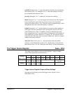
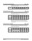
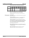
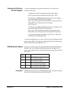

The Memory Control Register base +21
16
The memory control register is a read/write register that controls the
operation of digitizer memory. The register bits are defined below.
Address 7 6 5 4 3 2 1 0
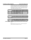
base + 02
16
128
64 32 16 8 4 2 1
Purpose
Backup
Enable
TTL Mux BNC Mux Address
Count
Enable
Memory
Read
Enable
Memory
Write
Enable
Setting
0 - OFF
1 - ON
0 - OFF
1 - ON
0 - reset
1 - enable
0 - reset
1 - enable
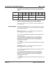
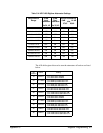
Memory Control Register Power-on/Reset Settings
At power-on or following a reset, the memory control register is set to
0011 1000 or 38
16
.
Bit Descriptions Backup Enable. Bit 7 is used to enable/disable the battery which maintains
memory at power-down.
TTL Mux and BNC Mux. Bit 6 and bits 5 - 3 are used by the digitizer’s
timebase processor. Their usage is not covered in this appendix.
Address Count Enable. Bit 2 is used to initialize the memory address
counter. Setting bit 2 to ’0’ disables the memory address counter but sets it
to receive the next memory address from the base address registers. Setting
bit 2 to ’1’ enables the address counter to receive addresses from the
terminal address register, thus allowing the counter to wrap around and
make repeated passes through memory.
Memory Read Enable. Setting bit 1 to ’1’ places digitizer memory in the
read mode. Data is placed on the internal high-speed bus if enabled by bits 1
- 0 of the traffic register.
Memory Write Enable. Bit 0 enables A/D readings to be written to
digitizer memory when bit 1 (memory read enable) is set to ’0’.
Appendix C Register Programming 365