DS33R11 Ethernet Mapper with Integrated T1/E1/J1 Transceiver
102 of 344
10.20.3 Transmitter
The transceiver uses a phase-lock loop along with a precision digital-to-analog converter (DAC) to create the
waveforms that are transmitted onto the E1 or T1 line. The waveforms created by the device meet the latest ETSI,
ITU-T, ANSI, and AT&T specifications. The user selects which waveform is generated by setting the ETS bit
(TR.LIC2.7) for E1 or T1 operation, then programming the L2/L1/L0 bits in register TR.LIC1 for the appropriate
application.
A 2.048MHz or 1.544MHz clock is required at TDCLKI for transmitting data presented at TPOSI and TNEGI.
Normally these pins are connected to TCLKO, TPOSO, and TNEGO. However, the LIU can operate in an
independent fashion. ITU specification G.703 requires an accuracy of ±50ppm for both T1 and E1. TR62411 and
ANSI specifications require an accuracy of ±32ppm for T1 interfaces. The clock can be sourced internally from
RCLKO or JACLK. See TR.LIC2.3, TR.LIC4.4, and TR.LIC4.5 for details. Because of the nature of the transmitter’s
design, very little jitter (less than 0.005UI
P-P
broadband from 10Hz to 100kHz) is added to the jitter present on
TCLKT. Also, the waveforms created are independent of the duty cycle of TCLKT. The transmitter in the device
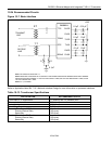
couples to the E1 or T1 transmit twisted pair (or coaxial cable in some E1 applications) through a 1:2 step-up
transformer. For the device to create the proper waveforms, the transformer used must meet the specifications
listed in
Table 10-13. The device has the option of using software-selectable transmit termination.
The transmit line drive has two modes of operation: fixed gain or automatic gain. In the fixed gain mode, the
transmitter outputs a fixed current into the network load to achieve a nominal pulse amplitude. In the automatic
gain mode, the transmitter adjusts its output level to compensate for slight variances in the network load. See the
Transmit Line Build-Out Control (TR.TLBC) register for details.
10.20.3.1 Transmit Short-Circuit Detector/Limiter
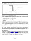
The device has an automatic short-circuit limiter that limits the source current to 50mA (RMS) into a 1Ω load. This
feature can be disabled by setting the SCLD bit (TR.LIC2.1) = 1. TCLE (TR.INFO2.5) provides a real-time
indication of when the current limiter is activated. If the current limiter is disabled, TCLE indicates that a short-
circuit condition exists. Status Register TR.SR1.2 provides a latched version of the information, which can be used
to activate an interrupt when enabled by the TR.IMR1 register. The TPD bit (TR.LIC1.0) powers down the transmit
line driver and three-states the TTIP and TRING pins.
10.20.3.2 Transmit Open-Circuit Detector
The device can also detect when the TTIP or TRING outputs are open circuited. TOCD (TR.INFO2.4) provides a
real-time indication of when an open circuit is detected. TR.SR1 provides a latched version of the information
(TR.SR1.1), which can be used to activate an interrupt when enabled by the TR.IMR1 register.
10.20.3.3 Transmit BPV Error Insertion
When IBPV (TR.LIC2.5) is transitioned from a 0 to a 1, the device waits for the next occurrence of three
consecutive 1s to insert a BPV. IBPV must be cleared and set again for another BPV error insertion.
10.20.3.4 Transmit G.703 Synchronization Signal (E1 Mode)
The transceiver can transmit the 2.048MHz square-wave synchronization clock as specified in Section 13 of ITU
G.703, October 1998. In order to transmit the 2.048MHz clock, when in E1 mode, set the transmit synchronization
clock enable (TR.LIC3.1) = 1.


