


DS33R11 Ethernet Mapper with Integrated T1/E1/J1 Transceiver
263 of 344
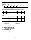
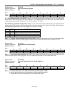
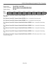
Register Name:
TR.RCBR2
Register Description:
Receive Channel Blocking Register 2
Register Address:
89h
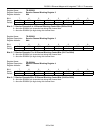
Bit # 7 6 5 4 3 2 1 0
Name CH16 CH15 CH14 CH13 CH12 CH11 CH10 CH9
Default 0 0 0 0 0 0 0 0
Bits 0 – 7: Receive Channels 9 to 16 Channel Blocking Control Bits (CH9 to CH16)
0 = force the RCHBLK pin to remain low during this channel time
1 = force the RCHBLK pin high during this channel time
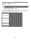
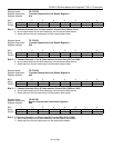
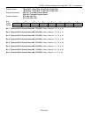
Register Name:
TR.RCBR3
Register Description:
Receive Channel Blocking Register 3
Register Address:
8Ah
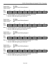
Bit # 7 6 5 4 3 2 1 0
Name CH24 CH23 CH22 CH21 CH20 CH19 CH18 CH17
Default 0 0 0 0 0 0 0 0
Bits 0 – 7: Receive Channels 17 to 24 Channel Blocking Control Bits (CH17 to CH24)
0 = force the RCHBLK pin to remain low during this channel time
1 = force the RCHBLK pin high during this channel time
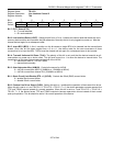
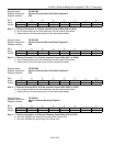
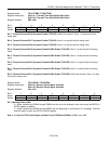
Register Name:
TR.RCBR4
Register Description:
Receive Channel Blocking Register 4
Register Address:
8Bh
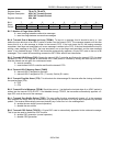
Bit # 7 6 5 4 3 2 1 0
Name CH32 CH31 CH30 CH29 CH28 CH27 CH26 CH25
Default 0 0 0 0 0 0 0 0
Bits 0 – 7: Receive Channels 25 to 32 Channel Blocking Control Bits (CH25 to CH32)
0 = force the RCHBLK pin to remain low during this channel time
1 = force the RCHBLK pin high during this channel time