


DS33R11 Ethernet Mapper with Integrated T1/E1/J1 Transceiver
103 of 344
10.21 MCLK Prescaler
A 16.384MHz, 8.192MHz, 4.096MHz, 2.048MHz, or 1.544MHz clock must be applied at MCLK. ITU specification
G.703 requires an accuracy of ±50ppm for both T1 and E1. TR62411 and ANSI specifications require an accuracy
of ±32ppm for T1 interfaces. A prescaler divides the 16MHz, 8MHz, or 4MHz clock down to 2.048MHz. There is an
on-board PLL for the jitter attenuator, which converts the 2.048MHz clock to a 1.544MHz rate for T1 applications.
Setting JAMUX (TR.LIC2.3) to a logic 0 bypasses this PLL.
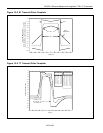
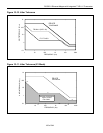
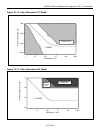
10.22 Jitter Attenuator
The device contains an on-board jitter attenuator that can be set to a depth of either 32 or 128 bits through the
JABDS bit (TR.LIC1.2). The 128-bit mode is used in applications where large excursions of wander are expected.
The 32-bit mode is used in delay-sensitive applications. The characteristics of the attenuation are shown in
Figure 10-12. The jitter attenuator can be placed in either the receive path or the transmit path by appropriately
setting or clearing the JAS bit (TR.LIC1.3). Setting the DJA bit (TR.LIC1.1) disables (in effect, removes) the jitter
attenuator. On-board circuitry adjusts either the recovered clock from the clock/data recovery block or the clock
applied at the TCLKT pin to create a smooth jitter-free clock that is used to clock data out of the jitter attenuator
FIFO. It is acceptable to provide a gapped/bursty clock at the TCLKT pin if the jitter attenuator is placed on the
transmit side. If the incoming jitter exceeds either 120UI
P-P
(buffer depth is 128 bits) or 28UI
P-P
(buffer depth is 32
bits), then the transceiver divides the internal nominal 32.768MHz (E1) or 24.704MHz (T1) clock by either 15 or 17
instead of the normal 16 to keep the buffer from overflowing. When the device divides by either 15 or 17, it also
sets the jitter attenuator limit trip (JALT) bit in Status Register 1 (TR.SR1.4).
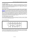
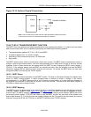
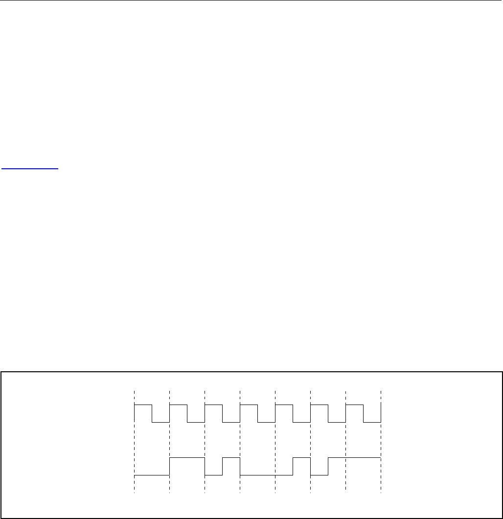
10.23 CMI (Code Mark Inversion) Option
The device provides a CMI interface for connection to optical transports. This interface is a unipolar 1T2B signal
type. Ones are encoded as either a logical 1 or 0 level for the full duration of the clock period. Zeros are encoded
as a 0-to-1 transition at the middle of the clock period.
Figure 10-6. CMI Coding
01 11001
CLOCK
DATA
CMI
Transmit and receive CMI are enabled through TR.LIC4.7. When this register bit is set, the TTIP pin outputs CMI-
coded data at normal levels. This signal can be used to directly drive an optical interface. When CMI is enabled,
the user can also use HDB3/B8ZS coding. When this register bit is set, the RTIP pin becomes a unipolar CMI
input. The CMI signal is processed to extract and align the clock with data.