DS33R11 Ethernet Mapper with Integrated T1/E1/J1 Transceiver
25 of 344
7 PIN DESCRIPTIONS
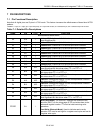
7.1 Pin Functional Description
Note that all digital pins are IO pins in JTAG mode. This feature increases the effectiveness of board level ATPG
patterns.
LEGEND: I = input, O = output, Ipu = input with pullup, Oz = output with tri-state, IO = bidirectional pin, IOz = bidirectional pin with tri-state.
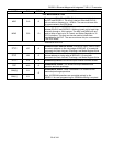
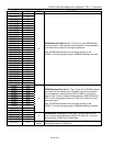
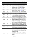
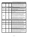
Table 7-1. Detailed Pin Descriptions
NAME PIN TYPE FUNCTION
MICROPROCESSOR PORT
A0 A18 I
Address Bit 0: Address bit 0 of the microprocessor interface.
Least Significant Bit.
A1 B18 I
Address Bit 1: Address bit 1 of the microprocessor interface.
A2 C18 I
Address Bit 2: Address bit 2 of the microprocessor interface.
A3 A17 I
Address Bit 3: Address bit 3 of the microprocessor interface.
A4 B17 I
Address Bit 4: Address bit 4 of the microprocessor interface.
A5 C17 I
Address Bit 5: Address bit 5 of the microprocessor interface.
A6 A16 I
Address Bit 6: Address bit 6 of the microprocessor interface.
A7 B16 I
Address Bit 7: Address bit 7 of the microprocessor interface.
A8 C16 I
Address Bit 8: Address bit 8 of the microprocessor interface.
A9 C15 I
Address Bit 9: Address bit 9 of the microprocessor interface.
D0 A14 IOZ
Data Bit 0: Bidirectional data bit 0 of the microprocessor interface.
Least Significant Bit. Not driven when CS =1 or RST = 0.
D1 B14 IOZ
Data Bit 1: Bidirectional data bit 1 of the microprocessor interface.
Not driven when CS = 1 or RST = 0.
D2 C14 IOZ
Data Bit 2: Bidirectional data bit 2 of the microprocessor interface.
Not driven when CS = 1 or RST = 0.
D3 A13 IOZ
Data Bit 3: Bidirectional data bit 3 of the microprocessor interface.
Not driven when CS = 1 or RST = 0.
D4 B13 IOZ
Data Bit 4: Bidirectional data bit 4 of the microprocessor interface.
Not driven when CS = 1 or RST = 0.
D5 C13 IOZ
Data Bit 5: Bidirectional data bit 5 of the microprocessor interface.
Not driven when CS = 1 or RST = 0.
D6 A12 IOZ
Data Bit 6: Bidirectional data bit 6 of the microprocessor interface.
Not driven when CS = 1 or RST = 0.
D7 B12 IOZ
Data Bit 7: Bidirectional data bit 7 of the microprocessor interface.
Most Significant Bit. Not driven when CS = 1 or RST = 0.
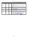
WR/RW
C11 I
Write (Intel Mode): The DS33R11 captures the contents of the
data bus (D0-D7) on the rising edge of WR and writes them to the
addressed register location. CS must be held low during write
operations.
Read Write (Motorola Mode): Used to indicate read or write
operation. RW must be set high for a register read cycle and low for
a register write cycle.


