DS33R11 Ethernet Mapper with Integrated T1/E1/J1 Transceiver
35 of 344
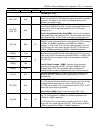
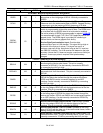
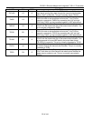
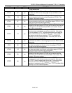
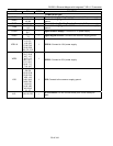
NAME PIN TYPE FUNCTION
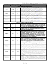
TDCLKO C2 O
Transmit Clock Output from the T1/E1/J1 Framer: Buffered
clock that is used to clock data through the transmit-side formatter
(either TCLKT or RDCLKI). This pin is normally tied to TDCLKI.
TNEGI C3 I
Transmit Negative-Data Input: Sampled on the falling edge of
TDCLKI for data to be transmitted out onto the T1 line. Can be
internally connected to TNEGO by connecting the LIUC pin high.
TPOSI and TNEGI can be connected together in NRZ applications.
TNEGO D3 O
Transmit Negative-Data Output: Updated on the rising edge of
TCLKO with the bipolar data out of the transmit-side formatter. This
pin is normally connected to TNEGI.
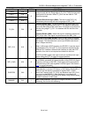
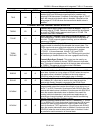
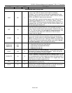
TPOSI B3 I
Transmit Positive-Data Input: Sampled on the falling edge of
TDCLKI for data to be transmitted out onto the T1 line. Can be
internally connected to TPOSO by connecting the LIUC pin high.
TPOSI and TNEGI can be connected together in NRZ applications.
TPOSO E1 O
Transmit Positive-Data Output: Updated on the rising edge of
TCLKO with the bipolar data out of the transmit-side formatter. Can
be programmed to source NRZ data by the output data format
(TR.IOCR1.0) control bit. This pin is normally connected to TPOSI.
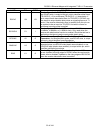
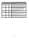
TDATA A4 I
Transmit Data: Sampled on the falling edge of TCLKT with data to
be clocked through the transmit-side formatter. This pin is normally
connected to TESO.
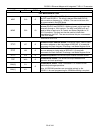
TESO D4 O
Transmit Elastic Store Output: Updated on the rising edge of
TCLKT with data out of the transmit-side elastic store whether the
elastic store is enabled or not. This pin is normally connected to
TDATA.


