


DS33R11 Ethernet Mapper with Integrated T1/E1/J1 Transceiver
45 of 344
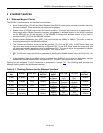
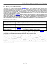
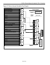
9.1.1 Ethernet Interface Clock Modes
The Ethernet PHY interface has several different clocking requirements, depending on the mode of operation.
Table 9-1 outlines the possible clocking modes for the Ethernet Interface. The buffered REF_CLKO output is
generated by division of the 100MHz system clock input by the user on SYSCLKI. The frequency of the
REF_CLKO pin is automatically determined by the DS33R11 based on the state of the RMIIMIIS pin. The
REF_CLKO function can be turned off with the
GL.CR1.RFOO bit. Note that in DCE and RMII operating modes,
the REF_CLKO signal should not be used to provide an input to REF_CLK, due to the reset requirements in these
operating modes.
In RMII mode, receive and transmit timing is always synchronous to a 50 MHz clock input on the REF_CLK pin.
The source of REF_CLK is expected to be the external PHY. The user has the option of using the 50MHz
REF_CLKO output as the timing source for the PHY. More information on RMII mode can be found in
Section
9.15.2.
While using MII mode with DTE operation, the MII clocks (RX_CLK and TX_CLK) are inputs that are expected to
be provided by the external PHY. While using MII mode with DCE operation, the MII clocks (TX_CLK and
RX_CLK) are output by the DS33R11, and are derived from the 25MHz REF_CLK input. More information on MII
mode can be found in Section
9.15.1.
9.1.2 Serial Interface Clock Modes
The serial interface timing is determined by the line clocks. Both the transmit and receive clocks (TCLKE and
RCLKI) are inputs, and can be gapped.