DS33R11 Ethernet Mapper with Integrated T1/E1/J1 Transceiver
27 of 344
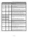
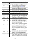
NAME PIN TYPE FUNCTION
MII/RMII PHY PORT
COL_DET N18 I
Collision Detect (MII): Asserted by the MAC PHY to indicate that a
collision is occurring. In DCE Mode this signal should be connected
to ground. This signal is only valid in half duplex mode, and is
ignored in full duplex mode.
RX_CRS/
CRS_DV
M19 I
Receive Carrier Sense (MII): Should be asserted (high) when data
from the PHY (RXD[3:0) is valid. For each clock pulse 4 bits arrive
from the PHY. Bit 0 is the least significant bit. In DCE mode,
connect to V
DD
.
Carrier Sense/Receive Data Valid (RMII): This signal is asserted
(high) when data is valid from the PHY. For each clock pulse 2 bits
arrive from the PHY. In DCE mode, this signal must be grounded.
RX_CLK M20 IO
Receive Clock (MII): Timing reference for RX_DV, RX_ERR and
RXD[3:0], which are clocked on the rising edge. RX_CLK frequency
is 25MHz for 100Mbit/s operation and 2.5MHz for 10Mbit/s
operation. In DTE mode, this is a clock input provided by the PHY.
In DCE mode, this is an output derived from REF_CLK providing
2.5MHz (10Mbit/s operation) or 25MHz (100Mbit/s operation).
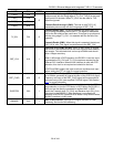
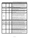
RXD[0] L18
RXD[1] L19
RXD[2] L20
RXD[3] M18
O
Receive Data 0 through 3 (MII): Four bits of received data,
sampled synchronously with the rising edge of RX_CLK. For every
clock cycle, the PHY transfers 4 bits to the DS33R11. RXD[0] is the
least significant bit of the data. Data is not considered valid when
RX_DV is low.
Receive Data 0 through 1 (RMII): Two bits of received data,
sampled synchronously with REF_CLK with 100Mbit/s mode.
Accepted when CRS_DV is asserted. When configured for
10Mbit/s mode, the data is sampled once every 10 clock periods.
RX_DV K19 I
Receive Data Valid (MII): This active high signal indicates valid
data from the PHY. The data RXD is ignored if RX_DV is not
asserted high.
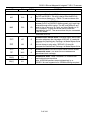
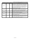
RX_ERR K18 I
Receive Error (MII): Asserted by the MAC PHY for one or more
RX_CLK periods indicating that an error has occurred. Active High
indicates Receive code group is invalid. If CRS_DV is low,
RX_ERR has no effect. This is synchronous with RX_CLK. In DCE
mode, this signal must be grounded.
Receive Error (RMII): Signal is synchronous to REF_CLK.
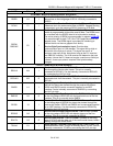
TX_CLK H19 IO
Transmit Clock (MII): Timing reference for TX_EN and TXD[3:0].
The TX_CLK frequency is 25MHz for 100Mbit/s operation and
2.5MHz for 10Mbit/s operation.
In DTE mode, this is a clock input provided by the PHY. In DCE
mode, this is an output derived from REF_CLK providing 2.5MHz
(10Mbit/s operation) or 25MHz (100Mbit/s operation).


