


DS33R11 Ethernet Mapper with Integrated T1/E1/J1 Transceiver
322 of 344
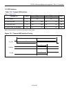
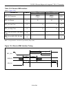
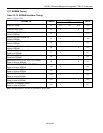
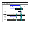
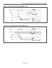
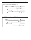
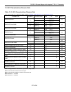
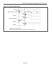
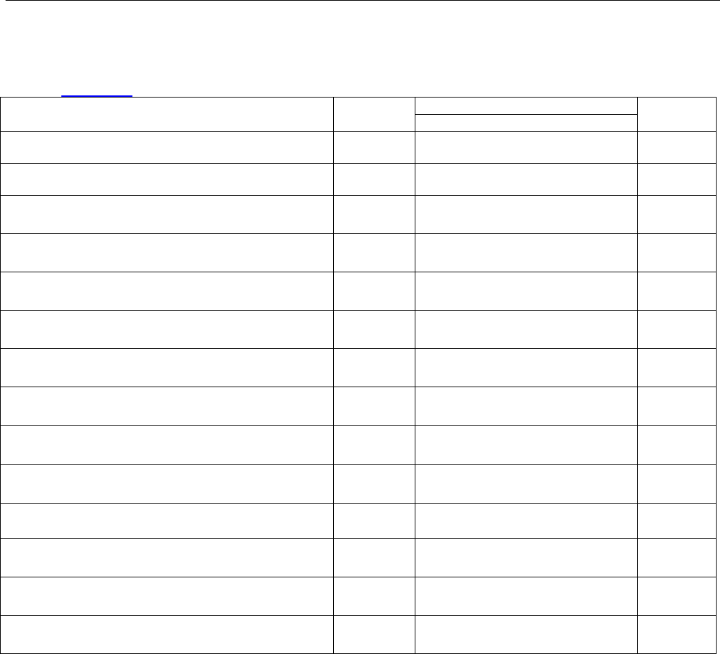
13.7 SDRAM Timing
Table 13-12. SDRAM Interface Timing
(Note 1, Figure 13-8)
100 MHz
PARAMETER SYMBOL
MIN TYP MAX
UNITS
SDCLKO Period
t1 9.7 10 10.3
ns
SDCLKO Duty Cycle t2 4 6
ns
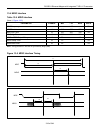
SDCLKO to SDATA Valid
Write to SDRAM
t3 7 ns
SDCLKO to SDATA Drive On
Write to SDRAM
t4 4 ns
SDCLKO to SDATA Invalid
Write to SDRAM
t5 3 ns
SDCLKO to SDATA Drive Off
Write to SDRAM
t6 4 ns
SDATA to SDCLKO Setup Time
Read from SDRAM
t7 2 ns
SDCLKO to SDATA Hold Time
Read from SDRAM
t8 2 ns
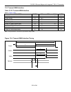
SDCLKO to SRAS, SCAS, SWE, SDCS Active
Read or Write to SDRAM
t9 5
ns
SDCLKO TO SRAS, SCAS, SWE, SDCS Inactive
Read or Write to SDRAM
t10 2
ns
SDCLKO to SDA, SBA Valid
Read or Write to SDRAM
t11 7
ns
SDCLKO TO SDA, SBA Invalid
Read or write to SDRAM
t12 2 ns
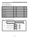
SDCLKO to SDMASK Valid
Read or write to SDRAM
t13 5 ns
SDCLKO TO SDMASK Invalid
Read or write to SDRAM
t14 2 ns
Note 1: Timing parameters in this table are guaranteed by design (GBD).